
 My Inquiry
 My Account


Analog Devices Inc./Maxim Integrated MAX367EWN+T
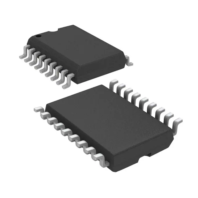
- Part No.:
- MAX367EWN+T
- Manufacturer:
- Analog Devices Inc./Maxim Integrated
- Category:
- Mixed Technology
- Package:
- 18-SOIC (0.295", 7.50mm Width)
- Datasheet:
-
 MAX367EWN+T.pdf
- Description:
- TVS DEVICE MIXED 40V 18SOIC
- Quantity:
- Payment:

- Shipping:

Inventory:918
Please send an inquiry. Send us your inquiry, and we will respond immediately.
Product details
Overview
MAX367EWN+T from Maxim Integrated is an 8-channel, two-terminal analog signal-line circuit protector IC designed for series insertion in sensitive analog interfaces. It operates with bipolar supplies (±2.25V to ±18V) or unipolar supplies (4.5V to 36V), delivers ≤100Ω on-resistance with power applied, limits fault current via voltage-dependent high-impedance transition, and protects against ±40V overvoltage events - used in data-acquisition front-ends, hot-insertion I/O modules, and redundant sensor interfaces.
For engineers reviewing the MAX367EWN+T datasheet, MAX367EWN+T pinout, MAX367EWN+T application, or MAX367EWN+T equivalent, key selection criteria include its symmetrical two-terminal architecture per channel, automatic fault clamping at ~1.3V below V+ or ~2.0V above V−, sub-1nA leakage at +25°C, open-circuit behavior with power off, and compatibility with high-impedance op-amp inputs without degrading signal integrity.
Technical Context
The MAX367EWN+T integrates eight independent, symmetrical MOSFET-based protector cells, each composed of two N-channel and one P-channel enhancement-mode FETs. Its protection mechanism relies on gate-threshold–driven conduction: under normal conditions (signal within ~1.5V of rails), all three FETs conduct to maintain low-resistance signal path; during overvoltage, gate bias loss forces high-impedance state without latch-up or polarity reversal.
No control logic, programming pins, or external biasing is required - operation is fully autonomous and supply-powered. Fault response is bidirectional and rail-referenced: output clamps to (V+ − 1.3V) for positive faults and (V− + 2.0V) for negative faults, with fault current flowing exclusively between IN/OUT terminals - zero current through V+/V− pins.
Key Specifications
| Parameter | Value and Actual Design Meaning |
|---|---|
| Channel count | 8 independent, interchangeable two-terminal protectors per device |
| Supply range | ±2.25V to ±18V (bipolar) or +4.5V to +36V (unipolar); supports single- or dual-supply systems |
| On-resistance | ≤100Ω max at ±10V supplies; ensures minimal signal attenuation in precision analog paths |
| Leakage current | <1nA max at +25°C with power on and no fault; preserves accuracy in µV-level measurements |
| Fault voltage limit | ±40V maximum differential across IN/OUT with V+/V− = 0V; survives worst-case power-off transients |
| Fault knee voltage | Clamps output to (V+ − 1.3V) or (V− + 2.0V); defines safe operating envelope for downstream circuitry |
| Signal bandwidth | Flat response to ≥5MHz in 50Ω systems; suitable for medium-speed data acquisition and ATE signals |
Pinout & Package
MAX367EWN+T is housed in a 18-pin Wide SO (Small Outline) package, 0.300-inch body width, with standard JEDEC MS-013AC footprint. Pin 1 is top-left corner (notch/dot side), pin numbering proceeds counter-clockwise.
| Pin/Terminal | Circuit Role | Design Meaning |
|---|---|---|
| 1–3, 4–8 | Signal Inputs (IN1–IN3, IN4–IN8) | Eight bidirectional analog signal terminals; electrically identical to outputs; interchangeable per channel |
| 9 | V− | Negative supply rail connection; sets lower reference for bipolar operation and fault knee |
| 10–14 | Signal Outputs (OUT4–OUT8) | Outputs corresponding to IN4–IN8; functionally identical to inputs; no fixed directionality |
| 15–17 | Signal Outputs (OUT1–OUT3) | Outputs corresponding to IN1–IN3; symmetric with inputs; may be used as inputs if needed |
| 18 | V+ | Positive supply rail connection; sets upper reference for bipolar operation and fault knee |
Key Features
| Feature | Design Value |
|---|---|
| Automatic overvoltage protection | Zero-configuration, rail-referenced clamping without external components or firmware |
| Power-off isolation | Virtual open circuit (≥1000MΩ) with V+/V− = 0V; prevents backfeeding and cross-talk during system shutdown |
| Symmetrical terminal architecture | IN/OUT pins per channel are functionally identical; simplifies PCB layout and enables flexible routing |
| Ultra-low leakage | <1nA at +25°C ensures minimal error in high-Z sensor interfaces and precision ADC front-ends |
| Bipolar + unipolar support | Single device supports both ±15V industrial analog and +24V PLC I/O without redesign |
Applications
| Process Control Signal Conditioning | Hot-Swappable Sensor Interface |
|---|---|
|
Use Scenario: Analog voltage/current inputs from field transmitters (4–20mA, ±10V) connect to PLC analog input modules exposed to wiring faults and ground loops. IC Role / Device Role / Timing Role: Series-connected protector per channel; isolates ADC front-end during 35V transients induced by lightning-induced surges or relay coil flyback. Use Value: Prevents permanent damage to precision op-amps and SAR ADCs while maintaining ≤100Ω path resistance for <0.01% gain error. |
Use Scenario: Modular I/O cards inserted into live backplanes where signal lines may contact chassis or adjacent slots before power sequencing completes. IC Role / Device Role / Timing Role: Eight-channel guard on all analog inputs/outputs; blocks ±40V fault voltages during hot-insertion, regardless of V+/V− ramp timing. Use Value: Eliminates need for manual power-down before card replacement; enables true hot-swap capability in test and measurement racks. |
| Redundant Data Acquisition System | ATE Analog Channel Protection |
|
Use Scenario: Dual-path DAQ systems where primary and backup channels share common sensor wiring but must remain electrically isolated during fault events. IC Role / Device Role / Timing Role: Independent protector per channel on both paths; ensures fault on primary does not propagate to backup via shared cabling. Use Value: Maintains system uptime by containing faults to single channel/path; avoids cascading failure in safety-critical monitoring. |
Use Scenario: Automated test equipment switching analog stimulus/response signals between DUT and instrumentation under program control. IC Role / Device Role / Timing Role: Front-end guard on all analog I/O pins; withstands miswiring, ESD, and accidental 24V shorts during probe contact or fixture changeover. Use Value: Reduces test head downtime and calibration drift caused by damaged front-end amplifiers; extends maintenance intervals. |
Equivalent & Alternatives
The following parts are listed as comparable options for similar analog signal-line protection applications.
| Alternative Part | Technical Difference | Application Difference | Selection Advice |
|---|---|---|---|
| MAX367CPN+ | Same silicon, 18-pin Plastic DIP package; wider operating temp (0°C to +70°C) vs. −40°C to +85°C | Limited to commercial-grade environments; unsuitable for industrial enclosures with wide ambient swings | Select MAX367CPN+ only for lab-grade or non-temperature-critical prototypes where through-hole assembly is preferred. |
| MAX367EPN+ | Same silicon, 18-pin Plastic DIP; extended temp range (−55°C to +125°C); higher cost and longer lead time | Validated for aerospace, downhole, and military platforms requiring extreme thermal resilience | Choose MAX367EPN+ when operating beyond −40°C or above +85°C is mandatory; otherwise, MAX367EWN+T offers optimal cost/performance balance. |
Compared with MAX367CPN+ and MAX367EPN+, the MAX367EWN+T provides industrial-temperature reliability in surface-mount form factor with identical electrical performance - making it the default choice for volume production in factory automation, test equipment, and modular instrumentation where space, thermal cycling, and reflow compatibility matter.
Availability
MAX367EWN+T is available at Aetrix Electronics and suitable for process control systems, hot-insertion boards/systems, and data-acquisition systems requiring stable component supply across multi-year production cycles and industrial temperature operation.
Supply support for MAX367EWN+T includes scheduled delivery planning, volume procurement assistance, BOM continuity management, traceable sourcing, and lifecycle availability coordination for OEM customers, industrial embedded developers, connected-device designers, and electronics production programs.
Manufacturer
Maxim Integrated (now part of Analog Devices) designs precision analog, mixed-signal, and power management ICs for industrial, automotive, and communications applications - emphasizing robustness, integration, and low-power operation.
The MAX366/MAX367 family was engineered specifically for fault-tolerant analog signal routing in harsh environments, targeting applications where transient overvoltage, power sequencing uncertainty, and long-term reliability outweigh raw speed or ultra-low capacitance requirements.
FAQ
What is the maximum continuous fault voltage the MAX367EWN+T can withstand?
The MAX367EWN+T withstands up to ±40V differential between its IN and OUT terminals when V+ and V− are at 0V - the highest rated fault condition. With power applied, maximum fault voltage is supply-dependent: e.g., ±25V with ±15V supplies or ±35V with ±5V supplies. This rating is validated per Absolute Maximum Ratings table and applies regardless of power state.
Does the MAX367EWN+T require external components to operate?
No, the MAX367EWN+T requires no external resistors, capacitors, or control signals. It draws <1µA supply current and functions autonomously - V+ and V− provide both bias and protection reference. External surge suppressors (e.g., TVS diodes) may be used upstream for high-energy transients, but are not required for basic ±40V fault containment.
Can the input and output pins of each channel be swapped on the MAX367EWN+T?
Yes - every IN/OUT pair (e.g., IN1/OUT1, IN2/OUT2, etc.) is fully symmetrical and interchangeable. The device contains no internal directionality; pin labeling is for schematic clarity only. This allows flexible PCB routing and eliminates orientation constraints during layout.
What happens to signal integrity when the MAX367EWN+T is powered off?
When V+ and V− are at 0V, the MAX367EWN+T presents a virtual open circuit (>1000MΩ) between each IN/OUT pair. No DC path exists, and signals are fully isolated up to ±40V. There is no leakage-induced offset or loading - critical for preserving sensor bias points and preventing backfeeding in powered-down subsystems.
How does the MAX367EWN+T behave during power-up and power-down transitions?
During V+/V− ramp-up, the MAX367EWN+T remains in high-impedance (fault) state until supply exceeds the input voltage by ~1.5V; output then tracks input with ~1.3V/2.0V rail offset. During ramp-down, it reverts to open circuit before supplies reach 0V. No glitches, polarity reversals, or latch-up occur - verified in Typical Operating Characteristics curves.
MAX367EWN+T Specifications
- Product attributes
- Attribute value
- Manufacturer:
- Analog Devices Inc./Maxim Integrated
- Package/Case:
- 18-SOIC (0.295", 7.50mm Width)
- Series:
- -
- Packaging:
- Tape & Reel (TR)
- Product Status:
- Active
- Voltage - Clamping:
- ±40V
- Technology:
- Mixed Technology
- Number of Circuits:
- 8
- Applications:
- General Purpose
- Grade:
- -
- Qualification:
- -
- Mounting Type:
- Surface Mount
- Supplier Device Package:
- 18-SOIC
MAX367EWN+T FAQ
1.How can I place an order for MAX367EWN+T through Aetrix?
Please submit a Request for Quotation (RFQ) for MAX367EWN+T on Aetrix. Our sales agent will provide a competitive quotation and guide you through the order confirmation once you accept the terms.
2.Are the price and stock information for MAX367EWN+T reliable?
The price and inventory of MAX367EWN+T are updated periodically and may fluctuate due to market conditions. Stock and pricing data are typically refreshed every 24 hours. Quotation validity for MAX367EWN+T is usually 5 days.
3.What payment methods are accepted for MAX367EWN+T?
We accept Wire Transfer, PayPal, Credit Card, Western Union, MoneyGram, and Escrow for MAX367EWN+T transactions.
Note: Certain payment methods may incur a processing fee.
4.How is shipping managed for MAX367EWN+T?
MAX367EWN+T orders can be shipped via leading logistics carriers, including DHL, UPS, FedEx, TNT, or Registered Mail.
Once your MAX367EWN+T order is processed, you will receive an email with the shipment details and tracking number.
Note: Tracking information may take up to 24 hours to appear. Express delivery typically takes 3–5 business days.
5.How can I obtain technical support or documentation for MAX367EWN+T?
For technical support, including MAX367EWN+T datasheets, pinout diagrams, or application guidance, please contact our engineering support team. They can provide detailed documentation and assistance for your MAX367EWN+T requirements.
6.How does Aetrix verify that MAX367EWN+T is sourced from the original manufacturer or authorized distributors?
All MAX367EWN+T products on Aetrix are procured from qualified distributors and authorized channels. Our dedicated quality assurance team conducts strict verification, including traceability checks and, if necessary, third-party testing. This ensures that MAX367EWN+T meets industry standards.
7.What is the process for return or replacement of MAX367EWN+T?
All MAX367EWN+T units undergo pre-shipment inspection (PSI). If there is an issue with MAX367EWN+T, returns or replacements are accepted under the following conditions:
1.Quantity discrepancies, incorrect items, or visible external defects (such as breakage or corrosion), acknowledged by Aetrix.
2.The issue is reported within 90 days of delivery.
3.The MAX367EWN+T part is unused and in its original packaging.
Return procedure for MAX367EWN+T:
1.Submit a request within 90 days.
2.Obtain a Return Material Authorization (RMA) from Aetrix.
MAX367EWN+T Tags
-
ESD03A5V5R17V
Stackpole Electronics Inc
-
ESDU02A5V5R17V
Stackpole Electronics Inc
-
0603ESDA-MLP7
Eaton - Electronics Division
.jpg)
-
0603ESDA2-TR2
Eaton - Electronics Division
-
PS04LTVA1
Eaton - Electronics Division
.jpg)
-
0402ESDA-MLP1
Eaton - Electronics Division
.jpg)
-
0402ESDA-MLP7
Eaton - Electronics Division
-
TPD2S017DBVR
Texas Instruments
.jpg)
-
V2F105A150Y2EDP
KYOCERA AVX
-
82307050029
Würth Elektronik
-
NCP360SNT1G
onsemi
-
V2F118A400Y2EDP
KYOCERA AVX
Tech Hub

A practical engineering guide to 3.3V and 5V logic compatibility, input thresholds, resistor dividers, translator ICs, MOSFET level shifting, I2C pull-ups, timing limits and power-sequencing risks.

The 74HC595 uses push-pull logic outputs, while the TPIC6B595 uses 50 V open-drain DMOS sinks for higher-power loads. This guide compares timing, current limits, 3.3 V interfacing, load wiring, thermal…

The 74HC595 converts serial data into eight stable parallel outputs. This guide covers pin functions, shift and storage timing, OE and MR behavior, drive-current limits, cascading, voltage compatibilit…

A technical comparison of level-sensitive latches and edge-triggered flip-flops, covering timing windows, setup and hold limits, master–slave operation, time borrowing, race-through, HDL inference and…

A D latch stores one bit while Enable controls when data can pass. This reference covers gate-level operation, truth tables, transparency, setup and hold timing, LE versus OE, common ICs and practical …

An SR latch stores one bit through cross-coupled feedback. This engineering reference covers NOR and NAND implementations, truth tables, forbidden-state recovery, gated operation, switch debouncing, fa…

Latch circuits retain one bit through feedback. This technical reference covers SR and D latches, truth tables, transparency, timing limits, latch-versus-flip-flop behavior, applications and common log…

An engineering guide to LED driver operation, constant-current and constant-voltage outputs, linear and switching topologies, dimming, IC selection, calculations, replacement compatibility, and fault c…

Operational amplifier guide covering op amp basics, feedback, ideal vs real op amps, common configurations, buffer circuits, offset, bias current, gain-bandwidth, slew rate, rail-to-rail limits and sel…

Jumper cables guide covering safe connection order, red and black clamp placement, final ground connection, cable gauge, length, clamp quality, copper vs CCA cables, jump starter comparison and battery…


