
 My Inquiry
 My Account


Analog Devices Inc./Maxim Integrated MAX3880ECB+
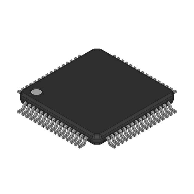
- Part No.:
- MAX3880ECB+
- Manufacturer:
- Analog Devices Inc./Maxim Integrated
- Category:
- Serializers, Deserializers
- Package:
- 64-TQFP Exposed Pad
- Datasheet:
-
 MAX3880ECB+.pdf
- Description:
- DESERIALIZER WITH CLOCK RECOVERY
- Quantity:
- Payment:

- Shipping:

Inventory:5,969
Please send an inquiry. Send us your inquiry, and we will respond immediately.
Product details
Overview
The MAX3880ECB+ from Maxim Integrated is a 2.488Gbps SDH/SONET 1:16 deserializer with integrated clock recovery, designed to convert high-speed serial NRZ data into 16-bit-wide 155Mbps LVDS parallel outputs for telecom transmission systems. It features a fully integrated PLL, operates from a single +3.3V supply, consumes 910mW, and supports system loopback diagnostics via dual serial inputs (SDI± and SLBI±).
For engineers reviewing the MAX3880ECB+ datasheet, MAX3880ECB+ pinout, MAX3880ECB+ application, or MAX3880ECB+ equivalent, this device is selected for precise jitter-critical SDH/SONET add/drop multiplexers, digital cross-connects, and timing-sensitive optical line interface designs requiring sub-0.46UIp-p jitter tolerance and >2000 consecutive identical digits handling.
Technical Context
The MAX3880ECB+ implements a fully differential architecture with an on-chip LC VCO running at 2.488GHz, phase/frequency detector, and digital frequency detector for rapid lock acquisition. Its PLL recovers clock from serial data without external reference, enabling retiming with <450ps clock-to-data delay variation across temperature.
It integrates dual LVDS input paths (main SDI± and diagnostic SLBI±), TTL-selectable signal routing (SIS), and LVDS synchronization inputs (SYNC±) that realign output data within two PCLK cycles by dropping one bit. The internal loop filter requires a 1.0µF capacitor between FIL+ and FIL− to set damping ratio.
Key Specifications
| Parameter | Value and Actual Design Meaning |
|---|---|
| Serial Data Rate | 2.488Gbps - matches OC-48/STM-16 line rate for SDH/SONET compliance |
| Parallel Output Rate | 155.52Mbps - provides 16-bit wide parallel bus synchronized to recovered clock |
| Jitter Tolerance | 0.46UIp-p (typ) at >10MHz - exceeds ITU-T G.823 and Bellcore GR-1378 requirements |
| Supply Voltage | +3.3V ±10% - single-rail operation simplifies power design in telecom line cards |
| Power Dissipation | 910mW (typ) - enables thermal management in dense 64-pin TQFP-EP packages |
| CID Tolerance | >2000 consecutive identical digits - ensures BER <1×10⁻¹⁰ under worst-case PRBS stress |
| Operating Temp | –40°C to +85°C - qualified for extended industrial and outdoor telecom environments |
Pinout & Package
MAX3880ECB+ is housed in a 64-pin TQFP-EP (exposed pad) package measuring 10mm × 10mm × 1.0mm, with the exposed pad soldered to PCB ground for thermal performance and EMI control.
| Pin/Terminal | Circuit Role | Design Meaning |
|---|---|---|
| SDI+, SDI− | Main Serial Data Input | Differential LVDS interface for primary 2.488Gbps OC-48 data stream |
| SLBI+, SLBI− | System Loopback Input | Secondary LVDS input for in-system diagnostics without external loopback hardware |
| SIS | Signal Input Select | TTL control pin selecting between SDI± (low) or SLBI± (high) as active data path |
| SYNC+, SYNC− | Synchronization Input | LVDS-aligned pulse input to shift parallel data alignment by 1 bit within ≤2 PCLK cycles |
| PCLK+, PCLK− | Parallel Clock Output | LVDS clock output referenced to recovered timing, used to latch PD0–PD15 data |
| PD0+ to PD15+ | Parallel Data Output (+) | 16-bit LVDS data bus updated on falling edge of PCLK; differential swing 250–400mVp-p |
| PD0− to PD15− | Parallel Data Output (−) | Complementary LVDS outputs requiring 100Ω differential termination per pair |
| FIL+, FIL− | PLL Loop Filter Interface | Connection points for external 1.0µF capacitor to stabilize PLL damping and jitter performance |
| PHADJ+, PHADJ− | Phase Adjustment Input | Differential voltage-controlled interface to fine-tune sampling point within data eye for optimal BER |
| LOL | Loss-of-Lock Monitor | TTL-active-low open-drain output indicating PLL unlock; valid only when serial data is present |
Key Features
| Feature | Design Value |
|---|---|
| Fully integrated clock recovery | Eliminates need for external clock source or separate PLL IC in SDH/SONET line interface cards |
| Dual serial input paths | Enables seamless system-level loopback testing without board-level signal rerouting or jumper changes |
| LVDS I/O with internal 100Ω termination | Reduces external component count for SYNC± inputs and simplifies layout for high-speed routing |
| Programmable phase alignment | Allows optimization of sampling point via PHADJ± to maximize margin against inter-symbol interference |
| Consecutive identical digit resilience | Maintains BER <1×10⁻¹⁰ over >2000-bit zero/one runs-critical for scrambled SONET overhead and payload |
Applications
| OC-48 Line Interface Card | Add/Drop Multiplexer (ADM) |
|---|---|
Use Scenario: Receiving 2.488Gbps OC-48 optical signal after PIN/TIA amplification and equalization. IC Role / Device Role / Timing Role: Deserializes and retimes incoming STM-16 frame into parallel 16-bit bus for FPGA-based framer processing. Use Value: Recovers clean clock from jittered serial stream, enabling sub-10⁻¹⁰ BER even with >0.4UIp-p input jitter. |
Use Scenario: Extracting and inserting tributary signals (e.g., VC-4) within a multi-rate ADM shelf. IC Role / Device Role / Timing Role: Converts backplane serial links to parallel data for time-slot interchange (TSI) matrix access. Use Value: Dual-input capability allows simultaneous monitoring of main and loopback paths during protection switching validation. |
| Digital Cross-Connect System (DCS) | SONET Test Equipment |
Use Scenario: Aggregating multiple OC-48 streams onto a high-capacity switch fabric. IC Role / Device Role / Timing Role: Provides deterministic latency and jitter-clean parallel interface to ASIC-based crosspoint controller. Use Value: Tight tCLK-Q spec (200–450ps) and low skew across PD0–PD15 ensure synchronous framing alignment across all ports. |
Use Scenario: Generating and analyzing compliant SDH/SONET waveforms in protocol analyzers or BERTs. IC Role / Device Role / Timing Role: Acts as reference deserializer in receiver test path with programmable sync and phase adjustment. Use Value: SYNC± inputs enable precise bit-slip injection for jitter tolerance measurement per ITU-T O.172. |
Equivalent & Alternatives
The following parts are listed as comparable options for similar deserializer-with-clock-recovery applications.
| Alternative Part | Technical Difference | Application Difference | Selection Advice |
|---|---|---|---|
| MAX3890ECB+ | Serializer companion; lacks deserialization function but shares pinout and loopback compatibility | Used in transceiver pairs where MAX3880ECB+ receives and MAX3890ECB+ transmits | Select MAX3890ECB+ only when building full bidirectional OC-48 link; not a functional replacement |
| LMH0384SQ/NOPB | 3.125Gbps HD-SDI deserializer; different data rate, no built-in PLL, requires external clock | Targeted at broadcast video, not telecom SDH/SONET; lacks LOL monitor and CID tolerance specs | Consider only for non-telecom high-speed serial-to-parallel conversion where jitter specs differ |
Compared with MAX3880ECB+, MAX3890ECB+ serves as its matched serializer partner rather than substitute, while LMH0384SQ/NOPB addresses broadcast video timing-not SDH/SONET compliance-making MAX3880ECB+ irreplaceable for telecom-grade jitter-critical line interfaces.
Availability
MAX3880ECB+ is available at Aetrix Electronics and suitable for OC-48 line interface cards, add/drop multiplexers, and digital cross-connect systems requiring stable component supply, long-term lifecycle support, and RoHS-compliant packaging.
Supply support for MAX3880ECB+ includes scheduled delivery planning, volume procurement assistance, BOM continuity management, traceable sourcing, and lifecycle availability coordination for OEM customers, industrial embedded developers, connected-device designers, and electronics production programs.
Manufacturer
Maxim Integrated (now part of Analog Devices) is a U.S.-based semiconductor company specializing in high-performance analog, mixed-signal, and RF solutions for communications, computing, and industrial markets.
The MAX3880ECB+ belongs to Maxim's high-speed communications product line, engineered specifically for SDH/SONET OC-48/STM-16 physical layer interfacing with emphasis on jitter performance, power efficiency, and system diagnostics.
FAQ
What is the primary function of the MAX3880ECB+ in SDH/SONET systems?
The MAX3880ECB+ functions as a 2.488Gbps serial-to-16-bit-parallel deserializer with integrated clock recovery. It extracts a synchronous clock from the incoming OC-48 serial data stream and retimes the data for reliable parallel transfer to framer or FPGA logic. Its jitter performance exceeds ITU-T G.823 and Bellcore GR-1378 standards, making it essential for telecom line interface cards where timing integrity is critical. The MAX3880ECB+ also supports system loopback diagnostics via its SLBI± inputs.
Does the MAX3880ECB+ require an external clock source?
No, the MAX3880ECB+ does not require an external clock source. It incorporates a fully integrated phase-locked loop (PLL) with an on-chip LC VCO operating at 2.488GHz, enabling autonomous clock recovery directly from the serial NRZ data input. This eliminates dependency on external timing references and simplifies system design in SDH/SONET equipment. The MAX3880ECB+ uses only a 1.0µF capacitor on FIL+/FIL− to configure loop dynamics.
How does the MAX3880ECB+ handle loss-of-lock detection?
The MAX3880ECB+ includes a dedicated TTL-compatible loss-of-lock (LOL) output (pin 63) that asserts low when the PLL loses frequency or phase lock. This signal has an internal 10kΩ pull-up resistor and responds within ~800ns after lock loss. Importantly, the LOL monitor is only valid when a serial data stream is present on SDI± or SLBI±; it does not indicate power failure or missing input signal. The MAX3880ECB+ specification confirms LOL validity is conditional on active data presence.
What is the purpose of the SYNC+ and SYNC− pins on the MAX3880ECB+?
The SYNC+ and SYNC− pins on the MAX3880ECB+ provide LVDS-synchronized bit-slip control to realign the parallel output word relative to the recovered clock. Applying a high pulse ≥4 serial bit periods (≥1.6ns) shifts data alignment by dropping one bit, guaranteeing realignment within two complete PCLK cycles. This feature enables precise frame boundary adjustment during system initialization or error recovery. The MAX3880ECB+ datasheet specifies SYNC functionality is implemented via internal LVDS receivers with 100Ω differential termination.
Can the MAX3880ECB+ operate with PECL-level inputs?
The MAX3880ECB+ accepts differential LVDS inputs (50–800mVp-p), not native PECL. To interface with PECL sources, external attenuation and AC-coupling are required-typically using a 25Ω series resistor per leg and 100Ω termination to VCC, as shown in Figure 7 of the MAX3880ECB+ datasheet. This preserves common-mode level and maintains 50Ω impedance matching. Direct PECL connection will exceed absolute maximum input voltage ratings and risk damage to the MAX3880ECB+.
MAX3880ECB+ Specifications
- Product attributes
- Attribute value
- Manufacturer:
- Analog Devices Inc./Maxim Integrated
- Series:
- -
- Package/Case:
- 64-TQFP Exposed Pad
- Packaging:
- Bulk
- Product Status:
- Active
- Function:
- Deserializer
- Data Rate:
- 2.488Gbps
- Input Type:
- Serial
- Output Type:
- LVDS
- Number of Inputs:
- 1
- Number of Outputs:
- 16
- Voltage - Supply:
- 3V ~ 3.6V
- Operating Temperature:
- -40°C ~ 85°C
- Grade:
- -
- Qualification:
- -
- Mounting Type:
- Surface Mount
- Supplier Device Package:
- 64-TQFP-EP (10x10)
MAX3880ECB+ FAQ
1.How can I place an order for MAX3880ECB+ through Aetrix?
Please submit a Request for Quotation (RFQ) for MAX3880ECB+ on Aetrix. Our sales agent will provide a competitive quotation and guide you through the order confirmation once you accept the terms.
2.Are the price and stock information for MAX3880ECB+ reliable?
The price and inventory of MAX3880ECB+ are updated periodically and may fluctuate due to market conditions. Stock and pricing data are typically refreshed every 24 hours. Quotation validity for MAX3880ECB+ is usually 5 days.
3.What payment methods are accepted for MAX3880ECB+?
We accept Wire Transfer, PayPal, Credit Card, Western Union, MoneyGram, and Escrow for MAX3880ECB+ transactions.
Note: Certain payment methods may incur a processing fee.
4.How is shipping managed for MAX3880ECB+?
MAX3880ECB+ orders can be shipped via leading logistics carriers, including DHL, UPS, FedEx, TNT, or Registered Mail.
Once your MAX3880ECB+ order is processed, you will receive an email with the shipment details and tracking number.
Note: Tracking information may take up to 24 hours to appear. Express delivery typically takes 3–5 business days.
5.How can I obtain technical support or documentation for MAX3880ECB+?
For technical support, including MAX3880ECB+ datasheets, pinout diagrams, or application guidance, please contact our engineering support team. They can provide detailed documentation and assistance for your MAX3880ECB+ requirements.
6.How does Aetrix verify that MAX3880ECB+ is sourced from the original manufacturer or authorized distributors?
All MAX3880ECB+ products on Aetrix are procured from qualified distributors and authorized channels. Our dedicated quality assurance team conducts strict verification, including traceability checks and, if necessary, third-party testing. This ensures that MAX3880ECB+ meets industry standards.
7.What is the process for return or replacement of MAX3880ECB+?
All MAX3880ECB+ units undergo pre-shipment inspection (PSI). If there is an issue with MAX3880ECB+, returns or replacements are accepted under the following conditions:
1.Quantity discrepancies, incorrect items, or visible external defects (such as breakage or corrosion), acknowledged by Aetrix.
2.The issue is reported within 90 days of delivery.
3.The MAX3880ECB+ part is unused and in its original packaging.
Return procedure for MAX3880ECB+:
1.Submit a request within 90 days.
2.Obtain a Return Material Authorization (RMA) from Aetrix.
MAX3880ECB+ Tags

-
SN65HVS880PWPR
Texas Instruments
-
SN65HVS882PWPR
Texas Instruments

-
FIN3386MTDX
onsemi
-
FIN3385MTDX
onsemi

-
SN65LV1023ARHBR
Texas Instruments

-
SN65LV1023ADBR
Texas Instruments
-
SN65LV1224BDBR
Texas Instruments

-
SN65LVDS93ADGGR
Texas Instruments
-
SN65LVDS93DGGR
Texas Instruments

-
TDES954RGZT
Texas Instruments
-
SN65LV1224BRHBT
Texas Instruments

-
DS90UB914QSQE/NOPB
Texas Instruments
Tech Hub

A practical engineering guide to 3.3V and 5V logic compatibility, input thresholds, resistor dividers, translator ICs, MOSFET level shifting, I2C pull-ups, timing limits and power-sequencing risks.

The 74HC595 uses push-pull logic outputs, while the TPIC6B595 uses 50 V open-drain DMOS sinks for higher-power loads. This guide compares timing, current limits, 3.3 V interfacing, load wiring, thermal…

The 74HC595 converts serial data into eight stable parallel outputs. This guide covers pin functions, shift and storage timing, OE and MR behavior, drive-current limits, cascading, voltage compatibilit…

A technical comparison of level-sensitive latches and edge-triggered flip-flops, covering timing windows, setup and hold limits, master–slave operation, time borrowing, race-through, HDL inference and…

A D latch stores one bit while Enable controls when data can pass. This reference covers gate-level operation, truth tables, transparency, setup and hold timing, LE versus OE, common ICs and practical …

An SR latch stores one bit through cross-coupled feedback. This engineering reference covers NOR and NAND implementations, truth tables, forbidden-state recovery, gated operation, switch debouncing, fa…

Latch circuits retain one bit through feedback. This technical reference covers SR and D latches, truth tables, transparency, timing limits, latch-versus-flip-flop behavior, applications and common log…

An engineering guide to LED driver operation, constant-current and constant-voltage outputs, linear and switching topologies, dimming, IC selection, calculations, replacement compatibility, and fault c…

Operational amplifier guide covering op amp basics, feedback, ideal vs real op amps, common configurations, buffer circuits, offset, bias current, gain-bandwidth, slew rate, rail-to-rail limits and sel…

Jumper cables guide covering safe connection order, red and black clamp placement, final ground connection, cable gauge, length, clamp quality, copper vs CCA cables, jump starter comparison and battery…


