
 My Inquiry
 My Account


Analog Devices Inc./Maxim Integrated MAX3891ECB
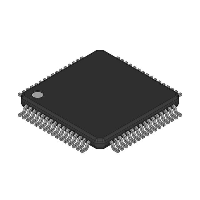
- Part No.:
- MAX3891ECB
- Manufacturer:
- Analog Devices Inc./Maxim Integrated
- Category:
- Serializers, Deserializers
- Package:
- 64-TQFP Exposed Pad
- Datasheet:
-
 MAX3891ECB.pdf
- Description:
- SDH/SONET, WITH CLOCK SYNTHESIS
- Quantity:
- Payment:

- Shipping:

Inventory:933
Please send an inquiry. Send us your inquiry, and we will respond immediately.
Product details
Overview
MAX3891ECB from Maxim Integrated is a 16:1 parallel-to-serial serializer IC for SDH/SONET transmission systems, converting 16-bit wide 155.52MHz parallel data into 2.5Gbps serial output using an integrated PLL clock synthesizer. It accepts single-ended LVPECL data inputs and delivers differential LVPECL serial data (SDO±) and clock (SCLKO±) outputs, operates from a single +3.3V supply, and supports extended temperature range (–40°C to +85°C) in a 64-pin TQFP-EP package.
For engineers reviewing the MAX3891ECB datasheet, MAX3891ECB pinout, MAX3891ECB application, or MAX3891ECB equivalent, this device is selected for high-speed telecom interface design where precise jitter performance (<3ps RMS), multi-rate reference clock support (38.88–155.52MHz), and system-level loopback diagnostics via CML SLBO± outputs are critical.
Technical Context
The MAX3891ECB implements a fully integrated phase/frequency detector, loop filter, voltage-controlled oscillator, and prescaler to synthesize a stable 2.488GHz internal serial clock from four selectable external reference frequencies. Its 16-bit parallel input register latches data on the rising edge of PCLKI±, while the 16-bit shift register retimes it against the synthesized SCLKO±.
Timing integrity is maintained via controlled skew (0–4ns) between PCLKO± (2.488GHz ÷ 16 = 155.52MHz) and PCLKI±, and setup/hold windows (300ps/700ps) referenced to PCLKI+ with 1ns rise/fall time. The CML loopback outputs (SLBO±) are enabled by TTL-level SOS and drive 50Ω terminated lines with 100–400mV differential swing.
Key Specifications
| Parameter | Value and Actual Design Meaning |
|---|---|
| Serial Data Rate | 2.488 Gbps - matches OC-48/STM-16 line rate for SDH/SONET compliance. |
| Parallel Input Clock | 155.52 MHz - standard SONET STS-3c/SDH STM-1 rate; also supports 77.76/51.84/38.88 MHz via CLKSET pin. |
| Supply Voltage | +3.3 V ±10% - single-rail operation simplifies power delivery in telecom line cards. |
| Output Jitter (RMS) | 3 ps - measured over 12kHz–20MHz bandwidth; ensures BER <10⁻¹² in optical links. |
| Power Consumption | 495 mW - enables thermal management in dense 64-pin TQFP-EP packages with exposed pad grounding. |
| Differential Output Swing | LVPECL: VOH = VCC−1.025V / VOL = VCC−1.81V; CML SLBO±: 100–400mV - defines signal integrity margins for 50Ω PECL/CML interconnects. |
| Operating Temperature | –40°C to +85°C - qualified for industrial and telecom infrastructure environments. |
Pinout & Package
Package: 64-pin TQFP with exposed pad (EP), 10mm × 10mm × 1mm body, RoHS-compliant, thermal pad soldered to PCB ground plane for electrical stability and heat dissipation.
| Pin/Terminal | Circuit Role | Design Meaning |
|---|---|---|
| GND (Pins 1,17,33,48,49,63) | Ground reference | Multiple dedicated ground pins minimize ground bounce across high-speed switching domains. |
| VCC (Pins 2,5,7,10,13,14,19,21,23,25,27,29,31,32,35,37,39,41,43,45,47,51,53,56,60,64) | +3.3V supply | 26 VCC pins provide low-impedance power distribution and decoupling for PECL/CML I/O banks. |
| PDI0–PDI15 (Pins 18,20,22,24,26,28,30,34,36,38,40,42,44,46,50,52) | Single-ended LVPECL parallel data inputs | 16-bit bus clocks on PCLKI+ rising edge; PDI15 transmitted first per serialization order. |
| SCLKO± (Pins 8,9) | Differential LVPECL serial clock output | 2.488GHz clock synchronized to SDO±; used for downstream deserializer timing recovery. |
| SDO± (Pins 11,12) | Differential LVPECL serial data output | 2.5Gbps output compliant with SONET OC-48 eye mask; requires 50Ω termination to (VCC−2V). |
| SLBO± (Pins 3,4) | CML system loopback outputs | Enabled by TTL SOS high; drives 50Ω to VCC for direct connection to MAX3881 deserializer loopback inputs. |
| RCLK± (Pins 57,58) | Differential LVPECL reference clock input | Accepts 38.88/51.84/77.76/155.52MHz; sets PLL multiplication ratio via CLKSET programming. |
| SOS (Pin 6) | TTL loopback enable input | Active-high control for SLBO±; allows in-system diagnostic testing without external loopback hardware. |
Key Features
| Feature | Design Value |
|---|---|
| Integrated PLL clock synthesis | Generates 2.488GHz serial clock from four standard telecom reference rates without external VCO or loop filter components. |
| Multi-rate reference clock support | Four selectable input frequencies (38.88/51.84/77.76/155.52MHz) configured via single CLKSET pin with resistor/GND/VCC options. |
| CML system loopback outputs | SLBO± outputs enable closed-loop diagnostics with MAX3881 deserializer, eliminating need for external test fixtures. |
| LVPECL I/O compatibility | Single-ended PDI inputs and differential SDO/SCLKO outputs simplify interface to legacy telecom ASICs and FPGAs. |
| Exposed-pad thermal management | 64-pin TQFP-EP package with soldered thermal pad achieves low junction-to-board thermal resistance for sustained 495mW operation. |
Applications
| 2.5Gbps SDH/SONET Transmission Systems | 2.5Gbps Access Nodes |
|---|---|
Use Scenario: Aggregating 16x E1/T1 streams into OC-48/STM-16 optical line interface. IC Role / Device Role / Timing Role: Serializer converts parallel overhead and payload data into 2.488Gbps serial stream synchronized to ITU-T G.707 clock hierarchy. Use Value: Meets ANSI T1.105, ITU-T G.957, and Bellcore GR-253 jitter specifications for carrier-grade optical transport. |
Use Scenario: Front-haul interface in DSLAM or GPON OLT chassis connecting ATM backplane to optical transceivers. IC Role / Device Role / Timing Role: Bridges FPGA-based packet processing logic to fiber-optic PHY layer using deterministic 155.52MHz parallel clock domain. Use Value: Enables plug-and-play interoperability with industry-standard deserializers (e.g., MAX3881) via SLBO± loopback capability. |
| Add/Drop Multiplexers | Digital Cross-Connects |
Use Scenario: Inserting/dropping tributary signals in SONET ADM shelf without disrupting line-rate continuity. IC Role / Device Role / Timing Role: Provides low-skew (0–4ns) PCLKO± output to synchronize overhead management circuitry with serialized payload. Use Value: Maintains frame alignment across multiple clock domains using internally derived PCLKO± from divided SCLKO±. |
Use Scenario: Reconfigurable grooming of DS3/E3 circuits in central office digital cross-connect systems. IC Role / Device Role / Timing Role: Converts parallel switch fabric data to serial line-side interface while preserving SONET section/line overhead structure. Use Value: Supports hot-swap redundancy and hitless reconfiguration via precise setup/hold timing (300ps/700ps) at 155.52MHz. |
Equivalent & Alternatives
The following parts are listed as comparable options for similar 16:1 serializer applications.
| Alternative Part | Technical Difference | Application Difference | Selection Advice |
|---|---|---|---|
| MAX3890ECB | Lacks integrated PLL; requires external 2.488GHz reference clock instead of multi-rate synthesis from lower-frequency inputs. | Used where board space permits discrete clock generation or when reference clock is already available at line rate. | Select MAX3890ECB only if external 2.488GHz clock source exists and CLKSET programmability is unnecessary. |
| DS25BR100TSQ | Supports 3.125Gbps (PCIe Gen1), not SONET-aligned 2.488Gbps; uses CML I/O, not LVPECL; no built-in loopback outputs. | Targeted at computing interconnects rather than telecom standards; lacks RCLK±/CLKSET flexibility and SLBO± diagnostics. | Choose DS25BR100TSQ only for non-telecom high-speed serial links requiring PCIe timing compliance. |
Compared with MAX3891ECB, MAX3890ECB eliminates clock synthesis complexity but increases BOM count and layout sensitivity, while DS25BR100TSQ offers higher raw speed but sacrifices SONET-specific features like multi-rate reference support, jitter compliance, and system-level loopback.
Availability
MAX3891ECB is available at Aetrix Electronics and suitable for 2.5Gbps SDH/SONET transmission systems, access node interfaces, add/drop multiplexers, and digital cross-connect equipment requiring stable component supply across extended temperature ranges and long product lifecycles.
Supply support for MAX3891ECB includes scheduled delivery planning, volume procurement assistance, BOM continuity management, traceable sourcing, and lifecycle availability coordination for OEM customers, industrial embedded developers, connected-device designers, and electronics production programs.
Manufacturer
Maxim Integrated (now part of Analog Devices) designs precision analog, mixed-signal, and high-speed interface ICs for industrial, communications, and computing applications.
The MAX3891ECB belongs to Maxim's high-speed telecom serializer family, engineered specifically for SONET/SDH OC-48 line-interface applications requiring integrated clock synthesis, low-jitter performance, and system-level diagnostics.
FAQ
What reference clock frequencies does the MAX3891ECB support?
The MAX3891ECB supports four differential LVPECL reference clock frequencies: 155.52MHz, 77.76MHz, 51.84MHz, and 38.88MHz. Selection is controlled by the CLKSET pin configuration-tied to VCC, open, 20kΩ to GND, or GND respectively. This enables flexible integration into various SONET/SDH timing hierarchies without external frequency dividers or synthesizers. The MAX3891ECB uses these inputs to generate its internal 2.488GHz serial clock via an integrated PLL.
How does the MAX3891ECB implement system loopback testing?
The MAX3891ECB provides dedicated CML loopback outputs (SLBO±) enabled by a TTL-level SOS input. When SOS is driven high, SLBO± deliver a copy of the internal serialized data path, allowing direct connection to a deserializer like the MAX3881 for end-to-end link validation. This eliminates external test equipment during manufacturing and field diagnostics. The MAX3891ECB's SLBO± outputs are internally terminated to 50Ω to VCC and require no additional biasing, simplifying loopback implementation.
What is the timing relationship between PCLKI± and PCLKO± in the MAX3891ECB?
In the MAX3891ECB, PCLKO± is the 155.52MHz output derived by dividing the internal 2.488GHz serial clock by 16. The allowable skew between PCLKO± and PCLKI± is 0ns to +4.0ns, meaning the PCLKI± rising edge must occur within that window after the PCLKO± rising edge to meet setup/hold requirements. This constraint ensures reliable latching of parallel data into the shift register. The MAX3891ECB's timing architecture guarantees this relationship across –40°C to +85°C.
Does the MAX3891ECB require external termination for its LVPECL outputs?
Yes, the MAX3891ECB's LVPECL outputs (SDO±, SCLKO±, PCLKO±) require external 50Ω termination to (VCC − 2V) for proper signal integrity and common-mode voltage compliance. The datasheet recommends either direct DC termination or Thevenin-equivalent networks (e.g., 82Ω/130Ω resistive divider) when (VCC − 2V) is unavailable. AC-coupling is permitted only when followed by appropriate DC termination. The MAX3891ECB itself does not integrate LVPECL output terminations.
What package type and thermal considerations apply to the MAX3891ECB?
The MAX3891ECB is housed in a 64-pin TQFP with exposed pad (EP), measuring 10mm × 10mm × 1mm. Its exposed thermal pad must be soldered directly to a PCB ground plane to ensure both electrical stability and thermal dissipation-critical for managing its 495mW power consumption. Thermal resistance is minimized through multiple VCC and GND pins (26 VCC, 6 GND), and the package is RoHS-compliant. The MAX3891ECB's thermal design enables reliable operation at full speed across –40°C to +85°C.
MAX3891ECB Specifications
- Product attributes
- Attribute value
- Manufacturer:
- Analog Devices Inc./Maxim Integrated
- Series:
- -
- Package/Case:
- 64-TQFP Exposed Pad
- Packaging:
- Bulk
- Product Status:
- Active
- Function:
- Serializer
- Data Rate:
- 2.5Gbps
- Input Type:
- LVPECL
- Output Type:
- PECL
- Number of Inputs:
- 16
- Number of Outputs:
- 1
- Voltage - Supply:
- 3V ~ 3.6V
- Operating Temperature:
- -40°C ~ 85°C (TA)
- Grade:
- -
- Qualification:
- -
- Mounting Type:
- Surface Mount
- Supplier Device Package:
- 64-TQFP-EP (10x10)
MAX3891ECB FAQ
1.How can I place an order for MAX3891ECB through Aetrix?
Please submit a Request for Quotation (RFQ) for MAX3891ECB on Aetrix. Our sales agent will provide a competitive quotation and guide you through the order confirmation once you accept the terms.
2.Are the price and stock information for MAX3891ECB reliable?
The price and inventory of MAX3891ECB are updated periodically and may fluctuate due to market conditions. Stock and pricing data are typically refreshed every 24 hours. Quotation validity for MAX3891ECB is usually 5 days.
3.What payment methods are accepted for MAX3891ECB?
We accept Wire Transfer, PayPal, Credit Card, Western Union, MoneyGram, and Escrow for MAX3891ECB transactions.
Note: Certain payment methods may incur a processing fee.
4.How is shipping managed for MAX3891ECB?
MAX3891ECB orders can be shipped via leading logistics carriers, including DHL, UPS, FedEx, TNT, or Registered Mail.
Once your MAX3891ECB order is processed, you will receive an email with the shipment details and tracking number.
Note: Tracking information may take up to 24 hours to appear. Express delivery typically takes 3–5 business days.
5.How can I obtain technical support or documentation for MAX3891ECB?
For technical support, including MAX3891ECB datasheets, pinout diagrams, or application guidance, please contact our engineering support team. They can provide detailed documentation and assistance for your MAX3891ECB requirements.
6.How does Aetrix verify that MAX3891ECB is sourced from the original manufacturer or authorized distributors?
All MAX3891ECB products on Aetrix are procured from qualified distributors and authorized channels. Our dedicated quality assurance team conducts strict verification, including traceability checks and, if necessary, third-party testing. This ensures that MAX3891ECB meets industry standards.
7.What is the process for return or replacement of MAX3891ECB?
All MAX3891ECB units undergo pre-shipment inspection (PSI). If there is an issue with MAX3891ECB, returns or replacements are accepted under the following conditions:
1.Quantity discrepancies, incorrect items, or visible external defects (such as breakage or corrosion), acknowledged by Aetrix.
2.The issue is reported within 90 days of delivery.
3.The MAX3891ECB part is unused and in its original packaging.
Return procedure for MAX3891ECB:
1.Submit a request within 90 days.
2.Obtain a Return Material Authorization (RMA) from Aetrix.
MAX3891ECB Tags

-
SN65HVS880PWPR
Texas Instruments
-
SN65HVS882PWPR
Texas Instruments

-
FIN3386MTDX
onsemi
-
FIN3385MTDX
onsemi

-
SN65LV1023ARHBR
Texas Instruments

-
SN65LV1023ADBR
Texas Instruments
-
SN65LV1224BDBR
Texas Instruments

-
SN65LVDS93ADGGR
Texas Instruments
-
SN65LVDS93DGGR
Texas Instruments

-
TDES954RGZT
Texas Instruments
-
SN65LV1224BRHBT
Texas Instruments

-
DS90UB914QSQE/NOPB
Texas Instruments
Tech Hub

A practical engineering guide to 3.3V and 5V logic compatibility, input thresholds, resistor dividers, translator ICs, MOSFET level shifting, I2C pull-ups, timing limits and power-sequencing risks.

The 74HC595 uses push-pull logic outputs, while the TPIC6B595 uses 50 V open-drain DMOS sinks for higher-power loads. This guide compares timing, current limits, 3.3 V interfacing, load wiring, thermal…

The 74HC595 converts serial data into eight stable parallel outputs. This guide covers pin functions, shift and storage timing, OE and MR behavior, drive-current limits, cascading, voltage compatibilit…

A technical comparison of level-sensitive latches and edge-triggered flip-flops, covering timing windows, setup and hold limits, master–slave operation, time borrowing, race-through, HDL inference and…

A D latch stores one bit while Enable controls when data can pass. This reference covers gate-level operation, truth tables, transparency, setup and hold timing, LE versus OE, common ICs and practical …

An SR latch stores one bit through cross-coupled feedback. This engineering reference covers NOR and NAND implementations, truth tables, forbidden-state recovery, gated operation, switch debouncing, fa…

Latch circuits retain one bit through feedback. This technical reference covers SR and D latches, truth tables, transparency, timing limits, latch-versus-flip-flop behavior, applications and common log…

An engineering guide to LED driver operation, constant-current and constant-voltage outputs, linear and switching topologies, dimming, IC selection, calculations, replacement compatibility, and fault c…

Operational amplifier guide covering op amp basics, feedback, ideal vs real op amps, common configurations, buffer circuits, offset, bias current, gain-bandwidth, slew rate, rail-to-rail limits and sel…

Jumper cables guide covering safe connection order, red and black clamp placement, final ground connection, cable gauge, length, clamp quality, copper vs CCA cables, jump starter comparison and battery…


