
 My Inquiry
 My Account


Analog Devices Inc./Maxim Integrated MAX3891ECB+D
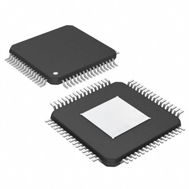
- Part No.:
- MAX3891ECB+D
- Manufacturer:
- Analog Devices Inc./Maxim Integrated
- Category:
- Serializers, Deserializers
- Package:
- 64-TQFP Exposed Pad
- Datasheet:
-
 MAX3891ECB+D.pdf
- Description:
- IC 16:1 SERIALIZER 64TQFP
- Quantity:
- Payment:

- Shipping:

Inventory:1,639
Please send an inquiry. Send us your inquiry, and we will respond immediately.
Product details
Overview
The MAX3891ECB+D from Maxim Integrated is a 16:1 parallel-to-serial serializer IC for SDH/SONET transmission systems, converting 16-bit wide 155.52MHz parallel data into a 2.488Gbps serial stream with integrated PLL-based clock synthesis, LVPECL-compatible I/O, and CML loopback outputs. It operates from a single +3.3V supply, consumes 495mW, and targets high-speed telecom backplane and add/drop multiplexer interfaces.
For engineers reviewing the MAX3891ECB+D datasheet, MAX3891ECB+D pinout, MAX3891ECB+D application, or MAX3891ECB+D equivalent, this device supports precise timing alignment in 2.5Gbps optical transport systems, requires careful PECL termination design, delivers sub-4ns PCLKO–PCLKI skew tolerance, and enables system-level diagnostics via TTL-controlled CML loopback.
Technical Context
The MAX3891ECB+D implements a fully integrated phase/frequency detector, loop filter/amplifier, voltage-controlled oscillator, and prescaler to synthesize a stable 2.488GHz serial clock from four selectable reference frequencies (38.88MHz to 155.52MHz). Its 16-bit parallel input register latches data on the rising edge of PCLKI, while the internal 16× divider generates PCLKO for overhead management circuitry.
Timing integrity relies on controlled skew between PCLKO and PCLKI (0–4ns), differential PECL signaling for SDO±/SCLKO±/PCLKO± outputs, and CML-compliant SLBO± outputs with 50Ω back-termination to VCC. The SOS TTL input enables/disables loopback without affecting core serialization functionality.
Key Specifications
| Parameter | Value and Actual Design Meaning |
|---|---|
| Serial Data Rate | 2.488Gbps - matches OC-48/STM-16 line rate for SDH/SONET compliance |
| Parallel Input Width & Rate | 16-bit @ 155.52MHz - supports full-rate ATM cell or SONET STS-3c payload mapping |
| Supply Voltage | +3.3V ±10% - single-rail operation simplifies power delivery in telecom line cards |
| Power Consumption | 495mW - enables thermal management in dense 64-pin TQFP-EP packages |
| Output Jitter (RMS) | 3ps - meets ITU-T G.823/G.825 jitter generation limits for synchronous networks |
| Reference Clock Inputs | 38.88MHz / 51.84MHz / 77.76MHz / 155.52MHz - covers all standard SONET/SDH frame rates |
| Operating Temperature | -40°C to +85°C - qualified for extended industrial and outdoor telecom equipment environments |
Pinout & Package
The MAX3891ECB+D is housed in a 64-pin TQFP with exposed pad (EP), requiring soldering of the EP to a PCB ground plane for thermal and electrical performance. Pin count includes 16 parallel data inputs (PDI0–PDI15), dual differential clock I/Os (PCLKI±, RCLK±, PCLKO±, SCLKO±), serial data outputs (SDO±), CML loopback outputs (SLBO±), and dedicated control pins (SOS, CLKSET, FIL±).
| Pin/Terminal | Circuit Role | Design Meaning |
|---|---|---|
| GND (Pins 1,17,33,48,49,63) | Ground Reference | Low-impedance return path for PECL/CML signaling and power decoupling |
| VCC (25 pins) | +3.3V Supply | Distributed power rail with local 0.1µF bypassing required per VCC pin |
| PDI0–PDI15 (Pins 18–20,22,24,26,28,30,34,36,38,40,42,44,46,50,52) | Single-Ended PECL Data Inputs | Latched on PCLKI rising edge; PDI15 transmitted first in serialized stream |
| SCLKO± (Pins 8–9) | Differential PECL Serial Clock Output | 2.488GHz clock synchronized to SDO±; used for deserializer clock recovery |
| SDO± (Pins 11–12) | Differential PECL Serial Data Output | 2.488Gbps output compliant with PECL load standards (50Ω to VCC−2V) |
| SLBO± (Pins 3–4) | CML Loopback Outputs | Enabled only when SOS = high; drive 50Ω terminated lines directly to MAX3881 inputs |
| SOS (Pin 6) | TTL Loopback Enable Input | Logic-high activates SLBO±; logic-low disables loopback without disrupting serialization |
| CLKSET (Pin 59) | Reference Clock Rate Selection | Configures RCLK frequency: VCC=155.52MHz, open=77.76MHz, 20kΩ-to-GND=51.84MHz, GND=38.88MHz |
Key Features
| Feature | Design Value |
|---|---|
| Integrated PLL clock synthesis | Eliminates external clock multiplier ICs and reduces BOM count in OC-48 line interface designs |
| Four selectable reference clock inputs | Supports interoperability across SONET OC-3/OC-12/OC-48 and SDH STM-1/STM-4/STM-16 systems |
| CML loopback outputs (SLBO±) | Enables real-time system diagnostics without external test equipment or signal rerouting |
| PECL-compatible I/O with 50Ω termination support | Ensures signal integrity over 10+ inch FR4 traces at 2.5Gbps with controlled impedance routing |
| 64-pin TQFP-EP package | Provides low thermal resistance for sustained 495mW operation in compact telecom modules |
Applications
| 2.5Gbps SDH/SONET Transmission Systems | 2.5Gbps Access Nodes |
|---|---|
Use Scenario: Line interface card in central office SONET ADM aggregating multiple DS3 feeds into OC-48. IC Role / Device Role / Timing Role: Serializer converts parallel overhead + payload data to serial OC-48 line rate with jitter-clean clock synthesis. Use Value: Meets Bellcore GR-253-CORE jitter accumulation requirements for long-haul network elements. |
Use Scenario: Fiber-to-the-curb (FTTC) node converting Ethernet frames to SONET for upstream transport. IC Role / Device Role / Timing Role: Bridges 155Mbps parallel bus from MAC layer to 2.488Gbps optical PHY with deterministic latency. Use Value: Enables seamless interworking between packet-switched access and circuit-switched core networks. |
| Add/Drop Multiplexers | Digital Cross-Connects |
Use Scenario: Reconfigurable ADM inserting/dropping VT1.5 tributaries within an OC-48 signal. IC Role / Device Role / Timing Role: Serializes processed tributary data for reinsertion using PCLKO-synchronized timing. Use Value: Maintains <4ns PCLKO–PCLKI skew to preserve SONET pointer alignment across drop/insert paths. |
Use Scenario: High-density DCS shelf performing non-blocking OC-48 grooming between multiple line cards. IC Role / Device Role / Timing Role: Converts parallel switch fabric output to serial line-side interface with low-jitter clock synthesis. Use Value: Achieves <3ps RMS jitter on SCLKO± to prevent bit errors during multi-stage switching cascades. |
Equivalent & Alternatives
The following parts are listed as comparable options for similar 2.5Gbps serializer applications.
| Alternative Part | Technical Difference | Application Difference | Selection Advice |
|---|---|---|---|
| MAX3890ECB+ | Same 64-pin TQFP-EP package and 2.488Gbps capability but lacks CML loopback outputs and SOS control | No built-in system diagnostic capability; requires external loopback path or separate test IC | Select when loopback testing is handled externally and cost reduction is prioritized |
| TI SN65LV1023AIPM | 16:1 serializer with 2.5Gbps rate but uses LVDS I/O instead of PECL and has no integrated PLL or reference clock flexibility | Requires external clock multiplier and level-shifting for PECL-based SONET PHYs | Select for LVDS-based backplanes where external clocking infrastructure already exists |
Compared with MAX3890ECB+, the MAX3891ECB+ adds essential CML loopback for field diagnostics; compared with SN65LV1023AIPM, it integrates clock synthesis and PECL compatibility, reducing component count and layout complexity in telecom line cards.
Availability
The MAX3891ECB+D is available at Aetrix Electronics and suitable for 2.5Gbps SDH/SONET transmission systems, digital cross-connects, add/drop multiplexers, and ATM backplanes requiring stable component supply across extended temperature ranges and long product lifecycles.
Supply support for MAX3891ECB+D includes scheduled delivery planning, volume procurement assistance, BOM continuity management, traceable sourcing, and lifecycle availability coordination for OEM customers, industrial embedded developers, connected-device designers, and electronics production programs.
Manufacturer
Maxim Integrated (now part of Analog Devices) designs precision analog, mixed-signal, and high-speed communication ICs for demanding industrial, telecom, and computing applications.
The MAX3891ECB+D belongs to Maxim's high-speed serializer family targeting OC-48/STM-16 optical transport equipment, with emphasis on jitter performance, protocol compliance, and system-level testability in carrier-grade hardware.
FAQ
What reference clock frequencies does the MAX3891ECB+D support?
MAX3891ECB+D supports four reference clock frequencies: 38.88MHz, 51.84MHz, 77.76MHz, and 155.52MHz. These are selected via the CLKSET pin using specific external connections (VCC, open, 20kΩ-to-GND, or GND). Each corresponds to standard SONET/SDH frame rates, enabling direct use in OC-3 through OC-48 systems without external clock multiplication. The MAX3891ECB+D synthesizes its internal 2.488GHz serial clock exclusively from these inputs.
How does the MAX3891ECB+D handle system-level diagnostics?
The MAX3891ECB+D provides built-in system loopback capability via CML-compatible SLBO± outputs, enabled by asserting TTL logic-high on the SOS pin. When active, SLBO± mirrors internal serialized data for direct connection to a deserializer like the MAX3881, enabling real-time link validation without external test gear. This function operates independently of main data flow, allowing diagnostics during live traffic. The MAX3891ECB+D does not require changes to serialization timing or configuration to activate loopback.
What is the maximum allowable skew between PCLKO and PCLKI in the MAX3891ECB+D?
The MAX3891ECB+D specifies a PCLKO-to-PCLKI skew range of 0ns to +4.0ns, meaning the PCLKI rising edge must occur no earlier than the PCLKO rising edge and no later than 4ns after it. This window ensures reliable latching of parallel data into the shift register. Exceeding this skew risks setup/hold violations and bit errors. The MAX3891ECB+D timing diagram (Figure 1) defines this relationship explicitly, and layout must maintain matched trace lengths to meet it.
Does the MAX3891ECB+D require external termination resistors for PECL I/O?
Yes, the MAX3891ECB+D requires external 50Ω termination to (VCC − 2V) for all PECL inputs and outputs (PCLKI±, RCLK±, PCLKO±, SCLKO±, SDO±) to ensure signal integrity at 2.5Gbps. The datasheet recommends either direct DC termination or Thevenin-equivalent networks (e.g., 82Ω/130Ω dividers) if (VCC − 2V) is unavailable. AC-coupling is permitted only when combined with proper DC termination. The MAX3891ECB+D itself does not integrate termination resistors.
What is the thermal management requirement for the MAX3891ECB+D package?
The MAX3891ECB+D uses a 64-pin TQFP with exposed pad (EP), and the EP must be soldered directly to a PCB ground plane with multiple thermal vias to dissipate 495mW reliably. Failure to connect the EP results in excessive junction temperature and potential reliability failure. Thermal resistance (θJA) depends on copper area and via count; Maxim recommends ≥400 mil² of 2oz copper under the EP with ≥9 vias (12mil diameter) for operation across −40°C to +85°C. The MAX3891ECB+D thermal performance is validated only with proper EP implementation.
MAX3891ECB+D Specifications
- Product attributes
- Attribute value
- Manufacturer:
- Analog Devices Inc./Maxim Integrated
- Series:
- -
- Package/Case:
- 64-TQFP Exposed Pad
- Packaging:
- Tray
- Product Status:
- Obsolete
- Function:
- Serializer
- Data Rate:
- 2.5Gbs
- Input Type:
- LVPECL
- Output Type:
- PECL
- Number of Inputs:
- 16
- Number of Outputs:
- 1
- Voltage - Supply:
- 3V ~ 3.6V
- Operating Temperature:
- -40°C ~ 85°C
- Grade:
- -
- Qualification:
- -
- Mounting Type:
- Surface Mount
- Supplier Device Package:
- 64-TQFP-EP (10x10)
MAX3891ECB+D FAQ
1.How can I place an order for MAX3891ECB+D through Aetrix?
Please submit a Request for Quotation (RFQ) for MAX3891ECB+D on Aetrix. Our sales agent will provide a competitive quotation and guide you through the order confirmation once you accept the terms.
2.Are the price and stock information for MAX3891ECB+D reliable?
The price and inventory of MAX3891ECB+D are updated periodically and may fluctuate due to market conditions. Stock and pricing data are typically refreshed every 24 hours. Quotation validity for MAX3891ECB+D is usually 5 days.
3.What payment methods are accepted for MAX3891ECB+D?
We accept Wire Transfer, PayPal, Credit Card, Western Union, MoneyGram, and Escrow for MAX3891ECB+D transactions.
Note: Certain payment methods may incur a processing fee.
4.How is shipping managed for MAX3891ECB+D?
MAX3891ECB+D orders can be shipped via leading logistics carriers, including DHL, UPS, FedEx, TNT, or Registered Mail.
Once your MAX3891ECB+D order is processed, you will receive an email with the shipment details and tracking number.
Note: Tracking information may take up to 24 hours to appear. Express delivery typically takes 3–5 business days.
5.How can I obtain technical support or documentation for MAX3891ECB+D?
For technical support, including MAX3891ECB+D datasheets, pinout diagrams, or application guidance, please contact our engineering support team. They can provide detailed documentation and assistance for your MAX3891ECB+D requirements.
6.How does Aetrix verify that MAX3891ECB+D is sourced from the original manufacturer or authorized distributors?
All MAX3891ECB+D products on Aetrix are procured from qualified distributors and authorized channels. Our dedicated quality assurance team conducts strict verification, including traceability checks and, if necessary, third-party testing. This ensures that MAX3891ECB+D meets industry standards.
7.What is the process for return or replacement of MAX3891ECB+D?
All MAX3891ECB+D units undergo pre-shipment inspection (PSI). If there is an issue with MAX3891ECB+D, returns or replacements are accepted under the following conditions:
1.Quantity discrepancies, incorrect items, or visible external defects (such as breakage or corrosion), acknowledged by Aetrix.
2.The issue is reported within 90 days of delivery.
3.The MAX3891ECB+D part is unused and in its original packaging.
Return procedure for MAX3891ECB+D:
1.Submit a request within 90 days.
2.Obtain a Return Material Authorization (RMA) from Aetrix.
MAX3891ECB+D Tags

-
SN65HVS880PWPR
Texas Instruments
-
SN65HVS882PWPR
Texas Instruments

-
FIN3386MTDX
onsemi
-
FIN3385MTDX
onsemi

-
SN65LV1023ARHBR
Texas Instruments

-
SN65LV1023ADBR
Texas Instruments
-
SN65LV1224BDBR
Texas Instruments

-
SN65LVDS93ADGGR
Texas Instruments
-
SN65LVDS93DGGR
Texas Instruments

-
TDES954RGZT
Texas Instruments
-
SN65LV1224BRHBT
Texas Instruments

-
DS90UB914QSQE/NOPB
Texas Instruments
Tech Hub

A practical engineering guide to 3.3V and 5V logic compatibility, input thresholds, resistor dividers, translator ICs, MOSFET level shifting, I2C pull-ups, timing limits and power-sequencing risks.

The 74HC595 uses push-pull logic outputs, while the TPIC6B595 uses 50 V open-drain DMOS sinks for higher-power loads. This guide compares timing, current limits, 3.3 V interfacing, load wiring, thermal…

The 74HC595 converts serial data into eight stable parallel outputs. This guide covers pin functions, shift and storage timing, OE and MR behavior, drive-current limits, cascading, voltage compatibilit…

A technical comparison of level-sensitive latches and edge-triggered flip-flops, covering timing windows, setup and hold limits, master–slave operation, time borrowing, race-through, HDL inference and…

A D latch stores one bit while Enable controls when data can pass. This reference covers gate-level operation, truth tables, transparency, setup and hold timing, LE versus OE, common ICs and practical …

An SR latch stores one bit through cross-coupled feedback. This engineering reference covers NOR and NAND implementations, truth tables, forbidden-state recovery, gated operation, switch debouncing, fa…

Latch circuits retain one bit through feedback. This technical reference covers SR and D latches, truth tables, transparency, timing limits, latch-versus-flip-flop behavior, applications and common log…

An engineering guide to LED driver operation, constant-current and constant-voltage outputs, linear and switching topologies, dimming, IC selection, calculations, replacement compatibility, and fault c…

Operational amplifier guide covering op amp basics, feedback, ideal vs real op amps, common configurations, buffer circuits, offset, bias current, gain-bandwidth, slew rate, rail-to-rail limits and sel…

Jumper cables guide covering safe connection order, red and black clamp placement, final ground connection, cable gauge, length, clamp quality, copper vs CCA cables, jump starter comparison and battery…


