
 My Inquiry
 My Account


Analog Devices Inc./Maxim Integrated MAX3949ETE+T
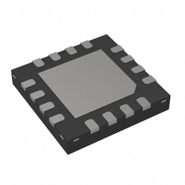
- Part No.:
- MAX3949ETE+T
- Manufacturer:
- Analog Devices Inc./Maxim Integrated
- Category:
- Laser Drivers
- Package:
- 16-WFQFN Exposed Pad
- Datasheet:
-
 MAX3949ETE+T.pdf
- Description:
- IC LASER DRV 11.3GB 3.63V 16TQFN
- Quantity:
- Payment:

- Shipping:

Inventory:4,425
Please send an inquiry. Send us your inquiry, and we will respond immediately.
Product details
Overview
The MAX3949ETE+T from Maxim Integrated is a 3.3V, 11.3Gbps AC-coupled laser diode driver IC optimized for SFP+ optical transceivers in 10GBASE-LR/LRM and OC192-SR systems. It delivers up to 85mA modulation current into a 5Ω differential load with 22ps edge speed (20%–80%), supports programmable bias current up to 105mA, and integrates on-chip 50Ω input termination and back-termination outputs for direct TOSA interfacing.
For engineers reviewing the MAX3949ETE+T datasheet, MAX3949ETE+T pinout, MAX3949ETE+T application, or MAX3949ETE+T equivalent, this device is selected for high-speed fiber-optic transmitter designs requiring low-power operation, deterministic jitter <13psP-P at 11.3Gbps, integrated eye safety monitoring, and 3-wire digital configurability without external passive components.
Technical Context
The MAX3949ETE+T implements a fully differential signal path with on-chip 50Ω AC-coupled input termination and 25Ω output back-termination, enabling direct drive of unmatched 5Ω–10Ω TOSAs via 25Ω flex circuits. Its input equalization block compensates host connector losses, while the dual 9-bit DACs independently control bias (IBIAS) and modulation (IMOD) currents with 200µA and 247µA LSB resolution respectively.
Timing-critical functions-including power-on reset (2.75V enable threshold), DISABLE-controlled fault latching (<3µs disable assert time), and FAULT recovery (<12µs) -are hardware-synchronized. The 3-wire interface (SDA/SCL/CSEL) supports four-device addressing via VSEL voltage levels and provides register-level access to TXEQ, TXDE, polarity, and diagnostic status bits.
Key Specifications
| Parameter | Value and Actual Design Meaning |
|---|---|
| Data Rate | Up to 11.3Gbps - supports full SFF-8431 SFP+ MSA compliance including 10.3125Gbps (10GBASE-R) and 11.3Gbps (OC192-SR). |
| Modulation Current | 10–85mAP-P into 5Ω load - enables precise laser extinction ratio tuning across temperature and aging without external current-setting resistors. |
| Bias Current | 5–105mA programmable - provides headroom for laser threshold drift and ensures stable CW operation under varying thermal conditions. |
| Edge Speed | 22ps (20%–80%) - achieves clean 11.3Gbps electrical eye opening with <13psP-P deterministic jitter using internal deemphasis. |
| Supply Voltage | 2.95V–3.63V (VCC/VCCT) - operates within standard 3.3V ±10% rail tolerances while maintaining full performance across -40°C to +95°C. |
| Digital Interface | 3-wire I²C-compatible (400–1000kHz) - reduces PCB routing complexity versus parallel interfaces and enables real-time diagnostics via SFF-8472 registers. |
| Thermal Resistance | θJA = 48°C/W (4-layer board) - supports continuous 1667mW dissipation at +70°C ambient, critical for compact SFP+ module thermal design. |
Pinout & Package
MAX3949ETE+T is housed in a 3mm × 3mm, 16-pin TQFN package (exposed pad grounded) with 0.4mm pitch. The exposed pad (EP) must be soldered to PCB ground for thermal and electrical integrity.
| Pin/Terminal | Circuit Role | Design Meaning |
|---|---|---|
| 1, DISABLE | CMOS disable input | Internally pulled up to VCC (7.5kΩ); logic-high disables both bias and modulation currents within 3µs - primary hardware safety interlock. |
| 2, VSEL | Analog address select | Four-level voltage input (GND/VCC/3, 2VCC/3, VCC) sets ADDR[6:5] for multi-device 3-wire bus configuration - eliminates address jumpers. |
| 3, FAULT | Open-drain fault indicator | Latched high on hard faults (e.g., BIAS under-voltage, TOUT overcurrent); cleared only by toggling DISABLE - enables system-level fault isolation. |
| 4, BMON | Bias current monitor | Sources 1/104 × IBIAS - allows precision laser current verification using single external resistor, supporting SFF-8472 analog monitoring. |
| 5,8, VCCT | Output-stage supply | Separate 3.3V rail powers TOUT+/TOUT- drivers; decoupling required near pins to maintain 11.3Gbps signal integrity and minimize crosstalk. |
| 6,7, TOUT-, TOUT+ | Differential modulation outputs | 25Ω internally terminated to VCCT; deliver complementary AC-coupled current into TOSA anode/cathode - eliminates external matching networks. |
| 9, BIAS | Laser bias current output | Combined current return path and bias source; compliance voltage 0.9–2.1V - compatible with common cathode TOSA configurations. |
| 10, CSEL | Chip-select input | Starts/stops 3-wire command cycles; internally pulled down (75kΩ) - enables robust multi-drop bus operation with noise immunity. |
| 11, SDA | Serial data I/O | Bidirectional open-drain line with internal 75kΩ pullup; requires external 4.7kΩ–10kΩ pullup to VCC - supports SFF-8472 register reads/writes. |
| 12, SCL | Serial clock input | CMOS input with internal 75kΩ pulldown - defines timing for register access; supports up to 1MHz clock for fast configuration updates. |
| 13,16, VCC | Core/digital supply | 3.3V supply for DACs, logic, and interface; separate from VCCT to isolate analog output noise from digital switching. |
| 14,15, TIN+, TIN- | Differential data inputs | 50Ω on-chip AC-coupled termination; accepts 0.15–1.0VP-P signals - eliminates external termination resistors and saves board space. |
| EP | Exposed thermal pad | Must be connected to solid ground plane - provides primary thermal path (θJC = 10°C/W) and reduces EMI coupling. |
Key Features
| Feature | Design Value |
|---|---|
| Programmable Input Equalization | Adjustable 0–5.5dB boost at 5.16GHz via SET_TXEQ register - compensates FR4 trace and SFP+ cage losses to restore high-frequency signal integrity. |
| Integrated Eye Safety Monitoring | Dual-threshold fault detection on BIAS, TOUT+, TOUT-, and VCCT rails with maskable alerts - meets IEC 60825-1 Class 1 laser safety requirements. |
| DC-Coupled TOSA Drive | Unmatched 5Ω–10Ω laser impedance support via unique output architecture - eliminates need for external DC-blocking capacitors in TOSA interface. |
| On-Chip Bias Monitor (BMON) | Fixed 1/104 current scaling with ±5% gain stability - enables accurate real-time laser current measurement using one external resistor per module. |
| 3-Wire Address Flexibility | VSEL pin accepts four discrete voltage levels (GND, VCC/3, 2VCC/3, VCC) to assign unique addresses - allows up to four MAX3949ETE+T devices on shared bus without address conflicts. |
| Power-On Reset Protection | Hardware POR circuit holds TX_EN low until VCC ≥ 2.75V - prevents accidental laser emission during power ramp-up, critical for optical safety certification. |
Applications
| 10GBASE-LR SFP+ Transceivers | 10GBASE-LRM SFP+ Transceivers |
|---|---|
|
Use Scenario: Long-reach 10G Ethernet transmission over single-mode fiber up to 10km using DFB lasers. IC Role / Device Role / Timing Role: Laser driver providing precise 11.3Gbps modulation current with deterministic jitter <8psP-P and integrated bias control. Use Value: Enables full SFF-8431 compliance with minimal external components, reducing BOM cost and layout area in pluggable optics modules. |
Use Scenario: Multi-mode 10G Ethernet over legacy OM1/OM2 fiber up to 220m using VCSELs with enhanced modal bandwidth compensation. IC Role / Device Role / Timing Role: High-fidelity AC-coupled driver with programmable input equalization to counteract modal dispersion in short-reach links. Use Value: Compensates for host connector and fiber channel losses via on-chip EQ, eliminating need for external equalizer ICs or complex PCB tuning. |
| OC192-SR SONET Transceivers | SFP+ Digital Diagnostic Modules |
|
Use Scenario: SONET OC-192 (9.953Gbps) short-reach transmission in telecom central office equipment using FP or DFB lasers. IC Role / Device Role / Timing Role: Low-jitter, low-power laser driver meeting GR-468 reliability standards with extended -40°C to +95°C operation. Use Value: Delivers 9.95Gbps performance with <6psP-P DJ and 0.55psRMS RJ - exceeds SONET jitter masks without external clock cleanup. |
Use Scenario: Real-time monitoring of laser health and optical output power in SFP+ modules compliant with SFF-8472. IC Role / Device Role / Timing Role: Integrated BMON and FAULT reporting with register-accessible TXSTAT1/TXSTAT2 status bits. Use Value: Provides calibrated bias current readback (±4% accuracy) and fault logging - satisfies digital diagnostics requirements without additional ADC or microcontroller resources. |
Equivalent & Alternatives
The following parts are listed as comparable options for similar laser driver applications.
| Alternative Part | Technical Difference | Application Difference | Selection Advice |
|---|---|---|---|
| MAX3948ETE+T | Lower max data rate (10.3Gbps vs. 11.3Gbps); identical pinout, package, and 3-wire interface. | Valid for 10GBASE-SR/LR but not OC192-SR or 11.3Gbps protocols; lacks 11.3Gbps jitter characterization. | Select when 10.3Gbps is sufficient and cost optimization is prioritized - drop-in replacement with no layout change. |
| SY88315BLMG | Higher supply voltage (3.3V/5V dual-rail); 10.7Gbps max; different pinout and 4-wire SPI interface. | Requires PCB redesign and firmware adaptation; supports broader industrial temp range (-40°C to +105°C) but no SFF-8472 integration. | Choose for mixed-voltage systems or where extended temperature margin outweighs SFP+ compatibility and digital diagnostics. |
Compared with MAX3948ETE+T and SY88315BLMG, the MAX3949ETE+T uniquely combines 11.3Gbps capability, SFF-8431/8472 compliance, and integrated BMON/FAULT in a 3mm × 3mm footprint - making it the optimal choice for next-generation SFP+ modules targeting SONET OC192 and 10G Ethernet LR/LRM.
Availability
MAX3949ETE+T is available at Aetrix Electronics and suitable for 10GBASE-LR optical transceivers, OC192-SR SONET modules, and SFP+ digital diagnostic subsystems requiring stable component supply, long-term lifecycle support, and RoHS-compliant packaging.
Supply support for MAX3949ETE+T includes scheduled delivery planning, volume procurement assistance, BOM continuity management, traceable sourcing, and lifecycle availability coordination for OEM customers, industrial embedded developers, connected-device designers, and electronics production programs.
Manufacturer
Maxim Integrated (now part of Analog Devices) is a semiconductor company specializing in high-performance analog, mixed-signal, and RF solutions for communications, computing, and industrial markets.
The MAX3949ETE+T belongs to Maxim's optical interconnect product line, engineered specifically for SFP+/QSFP+ pluggable transceiver modules demanding low-power, high-speed laser driving with integrated safety and diagnostics.
FAQ
What is the maximum data rate supported by the MAX3949ETE+T?
The MAX3949ETE+T supports data rates up to 11.3Gbps, fully complying with OC192-SR SONET and 10GBASE-LRM Ethernet standards. It maintains deterministic jitter below 13psP-P and random jitter under 0.55psRMS across its operating range, validated at 11.3Gbps with PRBS23 patterns.
Does the MAX3949ETE+T require external termination resistors for its differential inputs?
No, the MAX3949ETE+T includes on-chip 50Ω differential termination for TIN+/TIN- inputs, eliminating the need for external resistors. This simplifies PCB layout, reduces component count, and ensures consistent impedance matching across process and temperature variations.
How does the BMON pin on the MAX3949ETE+T function in practice?
The BMON pin on the MAX3949ETE+T sources a current equal to IBIAS/104, allowing direct measurement of laser bias current using a single external resistor to ground. For example, with IBIAS = 60mA, BMON delivers ~577µA - generating 577mV across a 1kΩ resistor for easy ADC sampling per SFF-8472 requirements.
Can the MAX3949ETE+T drive unmatched TOSAs without external DC-blocking capacitors?
Yes, the MAX3949ETE+T's unique output stage supports DC-coupled drive of unmatched TOSAs with impedances from 5Ω to 10Ω. Its internal 25Ω pull-up to VCCT and differential current-source architecture eliminate the need for external DC-blocking capacitors, improving signal fidelity and reducing BOM cost.
What fault conditions trigger the FAULT pin on the MAX3949ETE+T?
The FAULT pin on the MAX3949ETE+T asserts high for hard faults including BIAS voltage <0.35V, TOUT+ or TOUT- voltage outside VCCT–1.88V to VCCT–1.45V, or VCCT–VCC mismatch >0.6V. These conditions indicate unsafe laser operation and require DISABLE toggle to clear the latched fault state.
MAX3949ETE+T Specifications
- Product attributes
- Attribute value
- Manufacturer:
- Analog Devices Inc./Maxim Integrated
- Series:
- -
- Package/Case:
- 16-WFQFN Exposed Pad
- Packaging:
- Tape & Reel (TR)
- Product Status:
- Active
- Type:
- Laser Diode Driver
- Data Rate:
- 11.3Gbps
- Number of Channels:
- 1
- Voltage - Supply:
- 2.95V ~ 3.63V
- Current - Supply:
- 55 mA
- Current - Modulation:
- 85mA
- Current - Bias:
- 105 mA
- Operating Temperature:
- -40°C ~ 95°C
- Grade:
- -
- Qualification:
- -
- Supplier Device Package:
- 16-TQFN (3x3)
- Mounting Type:
- Surface Mount
MAX3949ETE+T FAQ
1.How can I place an order for MAX3949ETE+T through Aetrix?
Please submit a Request for Quotation (RFQ) for MAX3949ETE+T on Aetrix. Our sales agent will provide a competitive quotation and guide you through the order confirmation once you accept the terms.
2.Are the price and stock information for MAX3949ETE+T reliable?
The price and inventory of MAX3949ETE+T are updated periodically and may fluctuate due to market conditions. Stock and pricing data are typically refreshed every 24 hours. Quotation validity for MAX3949ETE+T is usually 5 days.
3.What payment methods are accepted for MAX3949ETE+T?
We accept Wire Transfer, PayPal, Credit Card, Western Union, MoneyGram, and Escrow for MAX3949ETE+T transactions.
Note: Certain payment methods may incur a processing fee.
4.How is shipping managed for MAX3949ETE+T?
MAX3949ETE+T orders can be shipped via leading logistics carriers, including DHL, UPS, FedEx, TNT, or Registered Mail.
Once your MAX3949ETE+T order is processed, you will receive an email with the shipment details and tracking number.
Note: Tracking information may take up to 24 hours to appear. Express delivery typically takes 3–5 business days.
5.How can I obtain technical support or documentation for MAX3949ETE+T?
For technical support, including MAX3949ETE+T datasheets, pinout diagrams, or application guidance, please contact our engineering support team. They can provide detailed documentation and assistance for your MAX3949ETE+T requirements.
6.How does Aetrix verify that MAX3949ETE+T is sourced from the original manufacturer or authorized distributors?
All MAX3949ETE+T products on Aetrix are procured from qualified distributors and authorized channels. Our dedicated quality assurance team conducts strict verification, including traceability checks and, if necessary, third-party testing. This ensures that MAX3949ETE+T meets industry standards.
7.What is the process for return or replacement of MAX3949ETE+T?
All MAX3949ETE+T units undergo pre-shipment inspection (PSI). If there is an issue with MAX3949ETE+T, returns or replacements are accepted under the following conditions:
1.Quantity discrepancies, incorrect items, or visible external defects (such as breakage or corrosion), acknowledged by Aetrix.
2.The issue is reported within 90 days of delivery.
3.The MAX3949ETE+T part is unused and in its original packaging.
Return procedure for MAX3949ETE+T:
1.Submit a request within 90 days.
2.Obtain a Return Material Authorization (RMA) from Aetrix.
MAX3949ETE+T Tags
-
EPC21701
EPC
-
EPC21601
EPC
-
MAX3799ETJ+T
Analog Devices Inc./Maxim Integrated
-
AD9665ACPZ-REEL7
Analog Devices Inc.

-
MAX3740AETG+T
Analog Devices Inc./Maxim Integrated
-
MAX3795ETG+
Analog Devices Inc./Maxim Integrated

-
EPC21603
EPC
-
ONET8501VRGPT
Texas Instruments
-
MAX3738ETG+T
Analog Devices Inc./Maxim Integrated
-
SY88022ALMG-TR
Microchip Technology
-
ISL78365ARZ-T7A
Renesas
-
EPC21603ENGRT
EPC
Tech Hub

A practical engineering guide to 3.3V and 5V logic compatibility, input thresholds, resistor dividers, translator ICs, MOSFET level shifting, I2C pull-ups, timing limits and power-sequencing risks.

The 74HC595 uses push-pull logic outputs, while the TPIC6B595 uses 50 V open-drain DMOS sinks for higher-power loads. This guide compares timing, current limits, 3.3 V interfacing, load wiring, thermal…

The 74HC595 converts serial data into eight stable parallel outputs. This guide covers pin functions, shift and storage timing, OE and MR behavior, drive-current limits, cascading, voltage compatibilit…

A technical comparison of level-sensitive latches and edge-triggered flip-flops, covering timing windows, setup and hold limits, master–slave operation, time borrowing, race-through, HDL inference and…

A D latch stores one bit while Enable controls when data can pass. This reference covers gate-level operation, truth tables, transparency, setup and hold timing, LE versus OE, common ICs and practical …

An SR latch stores one bit through cross-coupled feedback. This engineering reference covers NOR and NAND implementations, truth tables, forbidden-state recovery, gated operation, switch debouncing, fa…

Latch circuits retain one bit through feedback. This technical reference covers SR and D latches, truth tables, transparency, timing limits, latch-versus-flip-flop behavior, applications and common log…

An engineering guide to LED driver operation, constant-current and constant-voltage outputs, linear and switching topologies, dimming, IC selection, calculations, replacement compatibility, and fault c…

Operational amplifier guide covering op amp basics, feedback, ideal vs real op amps, common configurations, buffer circuits, offset, bias current, gain-bandwidth, slew rate, rail-to-rail limits and sel…

Jumper cables guide covering safe connection order, red and black clamp placement, final ground connection, cable gauge, length, clamp quality, copper vs CCA cables, jump starter comparison and battery…


