
 My Inquiry
 My Account


Analog Devices Inc./Maxim Integrated MAX4211EETE
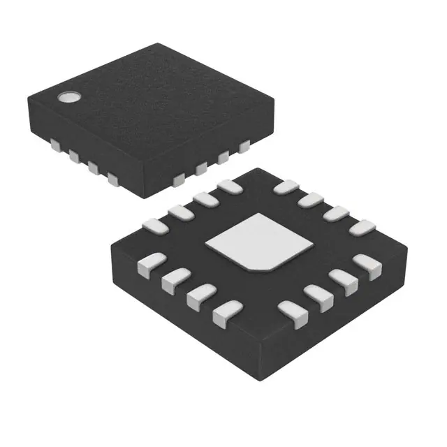
- Part No.:
- MAX4211EETE
- Manufacturer:
- Analog Devices Inc./Maxim Integrated
- Category:
- Current Regulation/Management
- Package:
- 16-WQFN Exposed Pad
- Datasheet:
-
 MAX4211EETE.pdf
- Description:
- IC CURRENT MONITOR 0.5% 16TQFN
- Quantity:
- Payment:

- Shipping:

Inventory:1,201
Please send an inquiry. Send us your inquiry, and we will respond immediately.
Product details
Overview
MAX4211EETE from Maxim Integrated is a high-side current and power monitor IC featuring integrated 1.21V bandgap reference, two open-drain comparators, and 25.00V/V current-sense gain. It delivers real-time analog outputs for load current (IOUT) and power (POUT), operates from +4V to +28V input common-mode voltage, supports +2.7V to +5.5V supply, and enables overpower/overcurrent detection in battery-powered systems.
For engineers reviewing the MAX4211EETE datasheet, MAX4211EETE pinout, MAX4211EETE application, or MAX4211EETE equivalent, this device is selected for high-accuracy, high-side sensing where ground-path integrity is critical-especially in smart battery packs, circuit-breaker protection, and power-supply instrumentation requiring ±1.5% current/power accuracy and comparator-driven fault response.
Technical Context
The MAX4211EETE integrates a precision high-side current-sense amplifier with 25.00V/V gain, a stable 1.21V reference, and two independent comparators with 5mV hysteresis and 4µs propagation delay. Its POUT output multiplies sensed current (via VSENSE) and source voltage (VIN), supporting external VIN routing for flexible power calculation architecture.
Designed for operation across –40°C to +85°C, it achieves 220kHz IOUT/POUT bandwidth, 80dB CMRR at DC, and 70dB PSRR, with open-drain comparator outputs rated to 28V-enabling direct interface to high-side MOSFET gate drivers in breaker applications without level-shifting.
Key Specifications
| Parameter | Value and Actual Design Meaning |
|---|---|
| Current-Sense Gain | 25.00V/V - sets IOUT = 25 × VSENSE, enabling precise current measurement with 100mV full-scale sense voltage |
| Power-Sense Gain | 25.00 1/V - configures POUT = 25 × VSENSE × VIN, supporting accurate power monitoring with 1V full-scale VIN range |
| Reference Voltage | 1.21V ±10mV - stable internal bandgap reference used by comparators and as system calibration anchor |
| Supply Voltage Range | +2.7V to +5.5V - compatible with standard 3.3V/5V logic supplies while maintaining full performance |
| Input Common-Mode Range | +4V to +28V - supports high-side sensing in 12V/24V industrial, automotive, and battery systems |
| Accuracy (Current/Power) | ±1.5% max - guaranteed total error over temperature, including gain, offset, and nonlinearity contributions |
| Comparator Outputs | Two open-drain, 28V-tolerant - allow wired-OR configuration and direct drive of external high-voltage switches |
Pinout & Package
MAX4211EETE is housed in a 16-pin TSSOP package (4.4mm × 5.0mm, 0.65mm pitch) with exposed thermal pad. Pin functions are validated per Maxim's official datasheet revision 1 (May 2005).
| Pin/Terminal | Circuit Role | Design Meaning |
|---|---|---|
| 1 (GND) | Ground Reference | Primary analog/digital return; connects to PCB ground plane and bypass capacitor |
| 2 (CIN1–) | Comparator 1 Inverting Input | Accepts threshold signal referenced to internal 1.21V; used for overcurrent detection |
| 3 (CIN1+) | Comparator 1 Non-Inverting Input | Accepts IOUT or POUT for comparison; enables programmable trip points |
| 4 (CIN2–) | Comparator 2 Inverting Input | Second threshold input; supports independent overvoltage or overpower detection |
| 5 (CIN2+) | Comparator 2 Non-Inverting Input | Accepts alternate output (e.g., POUT for overload, VIN for overvoltage) |
| 6 (LE) | Latch Enable | Active-high control that latches comparator outputs; prevents spurious trips during transients |
| 7 (INHIBIT) | Functional Disable | Active-high input that disables comparators and reduces quiescent current to <1µA |
| 8 (REF) | Reference Output | Provides buffered 1.21V reference for external circuitry or comparator thresholds |
| 9 (VCC) | Supply Voltage | +2.7V to +5.5V analog/digital supply; requires local 0.1µF ceramic bypass to GND |
| 10 (RS+) | High-Side Sense Input (+) | Connects to positive terminal of external sense resistor; handles up to +28V common-mode |
| 11 (RS–) | High-Side Sense Input (–) | Connects to load side of sense resistor; differential input with ±5V max rating |
| 12 (IOUT) | Current Output | Analog voltage proportional to load current (IOUT = 25 × VSENSE); rail-to-rail capable |
| 13 (POUT) | Power Output | Analog voltage proportional to load power (POUT = 25 × VSENSE × VIN); 220kHz bandwidth |
| 14 (COUT1) | Comparator 1 Output | Open-drain output; sinks ≥1mA at 0.6V; pulled up externally to ≤28V |
| 15 (COUT2) | Comparator 2 Output | Independent open-drain output; identical electrical specs to COUT1 |
| 16 (EP) | Exposed Thermal Pad | Internally connected to GND; must be soldered to PCB thermal plane for thermal reliability |
Key Features
| Feature | Design Value |
|---|---|
| Real-time dual-output monitoring | IOUT and POUT provide simultaneous, independent analog signals for current and power-eliminating need for external multipliers or microcontroller computation |
| ±1.5% current/power accuracy | Guaranteed over –40°C to +85°C, including gain error, offset, and multiplier nonlinearity-reducing calibration overhead in production |
| Integrated 1.21V reference | Stable, low-drift reference with ±10mV tolerance over temperature-serves as precision threshold source for both comparators |
| 28V-tolerant open-drain comparators | Enable direct interface to high-side N-channel MOSFET gates or optocouplers without level shifters-simplifying breaker control design |
| Low 670µA supply current | Minimizes self-heating and extends battery life in portable equipment; drops to <1µA in INHIBIT mode |
| 220kHz signal bandwidth | Supports fast transient detection (e.g., short-circuit events) with 10µs settling time-critical for responsive protection schemes |
Applications
| Overpower Circuit Breaker | Smart Battery Pack Monitoring |
|---|---|
|
Use Scenario: Detecting sustained overload conditions in 24V industrial power distribution panels to trigger automatic shutdown. IC Role / Device Role: High-side power monitor generating POUT proportional to VLOAD × ILOAD, fed into comparator with adjustable threshold. Use Value: Enables precise, temperature-stable trip points without external op-amps or ADCs-reducing BOM count and layout area. |
Use Scenario: Real-time current and energy tracking in Li-ion battery packs for state-of-charge (SoC) and health (SoH) estimation. IC Role / Device Role: Provides calibrated IOUT and POUT signals to MCU ADC, with REF used for ratiometric sensor scaling. Use Value: Delivers ±1.5% accuracy across –20°C to +60°C operating range-improving SoC estimation fidelity versus discrete solutions. |
| Short-Circuit Protection | Power-Supply Display |
|
Use Scenario: Sub-10µs response to sudden current surges in USB-C PD adapters to prevent MOSFET failure. IC Role / Device Role: IOUT drives comparator CIN1+; LE-latched output triggers gate driver disable within 4µs propagation delay. Use Value: Eliminates software latency; hardware-based protection ensures compliance with IEC 62368-1 fault response requirements. |
Use Scenario: Analog front-end for digital panel meters displaying real-time load power in telecom rectifiers. IC Role / Device Role: POUT provides direct voltage representation of watts consumed; REF stabilizes display scaling against supply variation. Use Value: Removes need for isolated current shunt amplifiers and multipliers-cutting cost and isolation complexity in AC/DC systems. |
Equivalent & Alternatives
The following parts are listed as comparable options for similar high-side power monitoring applications.
| Alternative Part | Technical Difference | Application Difference | Selection Advice |
|---|---|---|---|
| MAX4211DET | Uses external resistor-divider network; 16.67V/V current gain; lower full-scale sensitivity (150mV vs. 100mV) | Better suited for higher-current, lower-precision applications where design flexibility outweighs accuracy needs | Select when optimizing for cost-sensitive designs requiring adjustable gain via external resistors |
| MAX4211FET | 40.96V/V current gain; 100mV full-scale sense voltage; higher POUT offset error (30mV max vs. 20mV) | Preferred for ultra-low-current sensing (e.g., IoT standby monitoring) but less optimal for mid-range power ranges | Select when sensing sub-100mA loads where maximum gain improves SNR without sacrificing dynamic range |
Compared with MAX4211DET and MAX4211FET, the MAX4211EETE offers the optimal balance of accuracy (±1.5%), gain (25.00V/V), and offset performance (20mV max) for general-purpose 1A–10A power monitoring-making it the default choice for new designs targeting robustness and ease of use.
Availability
MAX4211EETE is available at Aetrix Electronics and suitable for smart battery packs, industrial circuit breakers, and power-supply instrumentation requiring stable component supply, long-term lifecycle support, and traceable sourcing.
Supply support for MAX4211EETE includes scheduled delivery planning, volume procurement assistance, BOM continuity management, traceable sourcing, and lifecycle availability coordination for OEM customers, industrial embedded developers, connected-device designers, and electronics production programs.
Manufacturer
Maxim Integrated (now part of Analog Devices) is a semiconductor company specializing in analog and mixed-signal ICs for power, sensing, and interface applications.
The MAX4211 series belongs to Maxim's high-side current/power monitor product line, designed specifically for accurate, ground-independent load monitoring in battery-powered and industrial systems.
FAQ
What is the function of the LE pin on the MAX4211EETE?
The LE (Latch Enable) pin on the MAX4211EETE is an active-high control that latches the comparator outputs (COUT1/COUT2) upon assertion, preventing false triggering during transient events. When LE is high, comparator outputs remain frozen at their last valid state until LE is deasserted. This feature is essential for reliable fault detection in noisy environments such as motor drives or switching power supplies, and is explicitly defined in the MAX4211EETE datasheet timing specifications.
Does the MAX4211EETE require external components for basic operation?
Yes-the MAX4211EETE requires a 0.1µF ceramic bypass capacitor between VCC and GND, an external sense resistor (RSENSE) between RS+ and RS–, and pull-up resistors on COUT1/COUT2 (typically 5kΩ to ≤28V). Unlike MAX4210 variants, it does not integrate a resistor divider, so VIN must be routed externally to POUT's multiplier input. These requirements are confirmed in the Functional Diagram and Absolute Maximum Ratings sections of the MAX4211EETE datasheet.
What is the maximum common-mode voltage the MAX4211EETE can handle on RS+ and RS–?
The MAX4211EETE supports a common-mode input voltage range of +4V to +28V on the RS+ pin, with differential input voltage limited to ±5V between RS+ and RS–. This allows direct high-side sensing in 24V systems without attenuation networks. The specification is guaranteed per Electrical Characteristics table (VCMR parameter) and validated across –40°C to +85°C for the MAX4211EETE variant.
How does the MAX4211EETE achieve ±1.5% power-sense accuracy?
The MAX4211EETE achieves ±1.5% total POUT output error through trimmed current-sense amplifier gain (25.00V/V), matched multiplier architecture, and factory-calibrated reference (1.21V ±10mV). Error includes contributions from gain nonlinearity, offset voltage (≤20mV), and temperature drift-all tested and binned during production. This accuracy is specified in the "Total POUT Output Error" row of the MAX4211EETE Electrical Characteristics table.
Can the MAX4211EETE operate from a 3.3V supply?
Yes-the MAX4211EETE operates from +2.7V to +5.5V on VCC, making it fully compatible with 3.3V systems. At 3.3V, it maintains full functionality: IOUT/POUT swing remains rail-to-rail, comparator outputs retain 28V tolerance, and accuracy stays within ±1.5% over temperature. Supply current increases slightly (to ~750µA typical), as documented in the "Supply Current vs. Supply Voltage" graph (toc01) of the MAX4211EETE datasheet.
MAX4211EETE Specifications
- Product attributes
- Attribute value
- Manufacturer:
- Analog Devices Inc./Maxim Integrated
- Series:
- -
- Package/Case:
- 16-WQFN Exposed Pad
- Packaging:
- Tube
- Product Status:
- Obsolete
- Function:
- Current Monitor
- Sensing Method:
- High-Side
- Accuracy:
- ±0.5%
- Voltage - Input:
- 4V ~ 28V
- Current - Output:
- -
- Operating Temperature:
- -40°C ~ 85°C
- Grade:
- -
- Qualification:
- -
- Mounting Type:
- Surface Mount
- Supplier Device Package:
- 16-TQFN (4x4)
MAX4211EETE FAQ
1.How can I place an order for MAX4211EETE through Aetrix?
Please submit a Request for Quotation (RFQ) for MAX4211EETE on Aetrix. Our sales agent will provide a competitive quotation and guide you through the order confirmation once you accept the terms.
2.Are the price and stock information for MAX4211EETE reliable?
The price and inventory of MAX4211EETE are updated periodically and may fluctuate due to market conditions. Stock and pricing data are typically refreshed every 24 hours. Quotation validity for MAX4211EETE is usually 5 days.
3.What payment methods are accepted for MAX4211EETE?
We accept Wire Transfer, PayPal, Credit Card, Western Union, MoneyGram, and Escrow for MAX4211EETE transactions.
Note: Certain payment methods may incur a processing fee.
4.How is shipping managed for MAX4211EETE?
MAX4211EETE orders can be shipped via leading logistics carriers, including DHL, UPS, FedEx, TNT, or Registered Mail.
Once your MAX4211EETE order is processed, you will receive an email with the shipment details and tracking number.
Note: Tracking information may take up to 24 hours to appear. Express delivery typically takes 3–5 business days.
5.How can I obtain technical support or documentation for MAX4211EETE?
For technical support, including MAX4211EETE datasheets, pinout diagrams, or application guidance, please contact our engineering support team. They can provide detailed documentation and assistance for your MAX4211EETE requirements.
6.How does Aetrix verify that MAX4211EETE is sourced from the original manufacturer or authorized distributors?
All MAX4211EETE products on Aetrix are procured from qualified distributors and authorized channels. Our dedicated quality assurance team conducts strict verification, including traceability checks and, if necessary, third-party testing. This ensures that MAX4211EETE meets industry standards.
7.What is the process for return or replacement of MAX4211EETE?
All MAX4211EETE units undergo pre-shipment inspection (PSI). If there is an issue with MAX4211EETE, returns or replacements are accepted under the following conditions:
1.Quantity discrepancies, incorrect items, or visible external defects (such as breakage or corrosion), acknowledged by Aetrix.
2.The issue is reported within 90 days of delivery.
3.The MAX4211EETE part is unused and in its original packaging.
Return procedure for MAX4211EETE:
1.Submit a request within 90 days.
2.Obtain a Return Material Authorization (RMA) from Aetrix.
MAX4211EETE Tags
.jpg)
-
PSSI2021SAY,115
Nexperia USA Inc.

-
BCR401RE6327HTSA1
Infineon Technologies

-
INA199B2DCKR
Texas Instruments
-
INA199A1DCKR
Texas Instruments
-
INA199B1DCKR
Texas Instruments
-
NSI45015WT1G
onsemi
-
NSI45020T1G
onsemi
-
NSI45030AT1G
onsemi
-
NSI45025AT1G
onsemi
-
NSI45020AT1G
onsemi
-
NSI50010YT1G
onsemi
-
LM334Z/NOPB
Texas Instruments
Tech Hub

A practical engineering guide to 3.3V and 5V logic compatibility, input thresholds, resistor dividers, translator ICs, MOSFET level shifting, I2C pull-ups, timing limits and power-sequencing risks.

The 74HC595 uses push-pull logic outputs, while the TPIC6B595 uses 50 V open-drain DMOS sinks for higher-power loads. This guide compares timing, current limits, 3.3 V interfacing, load wiring, thermal…

The 74HC595 converts serial data into eight stable parallel outputs. This guide covers pin functions, shift and storage timing, OE and MR behavior, drive-current limits, cascading, voltage compatibilit…

A technical comparison of level-sensitive latches and edge-triggered flip-flops, covering timing windows, setup and hold limits, master–slave operation, time borrowing, race-through, HDL inference and…

A D latch stores one bit while Enable controls when data can pass. This reference covers gate-level operation, truth tables, transparency, setup and hold timing, LE versus OE, common ICs and practical …

An SR latch stores one bit through cross-coupled feedback. This engineering reference covers NOR and NAND implementations, truth tables, forbidden-state recovery, gated operation, switch debouncing, fa…

Latch circuits retain one bit through feedback. This technical reference covers SR and D latches, truth tables, transparency, timing limits, latch-versus-flip-flop behavior, applications and common log…

An engineering guide to LED driver operation, constant-current and constant-voltage outputs, linear and switching topologies, dimming, IC selection, calculations, replacement compatibility, and fault c…

Operational amplifier guide covering op amp basics, feedback, ideal vs real op amps, common configurations, buffer circuits, offset, bias current, gain-bandwidth, slew rate, rail-to-rail limits and sel…

Jumper cables guide covering safe connection order, red and black clamp placement, final ground connection, cable gauge, length, clamp quality, copper vs CCA cables, jump starter comparison and battery…


