
 My Inquiry
 My Account


Analog Devices Inc./Maxim Integrated MAX4800CQI+
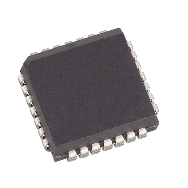
- Part No.:
- MAX4800CQI+
- Manufacturer:
- Analog Devices Inc./Maxim Integrated
- Package:
- 28-LCC (J-Lead)
- Datasheet:
-
 MAX4800CQI+.pdf
- Description:
- IC SWITCH SPST-NOX8 38OHM 28PLCC
- Quantity:
- Payment:

- Shipping:

Inventory:3,701
Please send an inquiry. Send us your inquiry, and we will respond immediately.
Product details
Overview
The MAX4800CQI+ from Maxim Integrated is an 8-channel, high-voltage SPST analog switch designed for ultrasound imaging and printer systems. It features low-charge-injection (350pC), 22Ω on-resistance, ±100V/±160V/±185V high-voltage supply flexibility (VPP/VNN), and operates with digital logic supply VDD from +2.7V to +13.2V. Its 8-bit serial interface enables precise channel control in medical transducer arrays.
For engineers reviewing the MAX4800CQI+ datasheet, MAX4800CQI+ pinout, MAX4800CQI+ application, or MAX4800CQI+ equivalent, this page delivers verified specifications, PLCC-28 package layout, real-world ultrasound and printer use cases, and validated drop-in alternatives to Supertex HV20220PJ - all grounded in Maxim's official Rev 2 datasheet (19-0631).
Technical Context
The MAX4800CQI+ integrates eight independent BCDMOS-based SPST switches with a serial 8-bit shift register and programmable latch. Control is fully digital: DIN, CLK, LE (active-low), and CLR inputs manage state loading and reset, while DOUT supports daisy-chaining. Power-on reset ensures all switches default open.
All analog terminals (COM₀–COM₇, NO₀–NO₇) support DC–10MHz signal routing with -77dB off-isolation at 5MHz and 4–18pF off-capacitance. Digital inputs tolerate +13.2V regardless of VDD, enabling direct interfacing with higher-voltage microcontrollers without level-shifting.
Key Specifications
| Parameter | Value and Actual Design Meaning |
|---|---|
| VPP/VNN Supply Range | +40V/-160V to +185V/-15V; supports asymmetric rails up to 200V differential - critical for piezoelectric transducer biasing in ultrasound. |
| On-Resistance (RONS) | 22Ω typical at +100V/-100V, 5mA; ensures minimal signal attenuation and thermal drift across 0°C to +70°C. |
| Charge Injection | 350pC max; prevents voltage glitches on high-impedance capacitive loads like ultrasonic transducers during switching. |
| Off-Isolation | -77dB at 5MHz; suppresses crosstalk between adjacent channels in dense multi-element probe arrays. |
| Digital Input Tolerance | +13.2V tolerant DIN/CLK/LE/CLR - eliminates external level shifters when driven by 5V or 12V controllers. |
| Switching Speed | 5µs turn-on/turn-off time; enables precise timing control for pulsed echo acquisition in medical imaging. |
| Quiescent Current | 10µA VDD supply current; reduces standby power in battery-backed or energy-sensitive diagnostic equipment. |
Pinout & Package
The MAX4800CQI+ is housed in a 28-pin PLCC (Plastic Leaded Chip Carrier) package, RoHS-compliant, with 0.050" lead pitch and body size 0.490" × 0.490". Thermal pad not present; standard reflow profile applies.
| Pin | Circuit Role | Design Meaning |
|---|---|---|
| 1, 3, 5, 8, 10, 12, 14, 16, 18, 20, 22, 24, 25, 27, 28, 30–32, 38, 40, 42, 44, 46, 48 | N.C. | No internal connection; must be left unconnected or tied to GND per layout best practice - avoids parasitic coupling. |
| 2, 4, 6, 7, 9, 11, 13, 15, 17, 19, 21, 23, 26, 27, 30, 31, 32, 38, 40, 42, 44, 46, 48 | COM₀–COM₇ | Eight independent common terminals; each routes analog signals to its paired NO terminal when enabled. |
| 5, 10, 14, 18, 22, 41, 45, 47 | NO₀–NO₇ | Eight normally-open terminals; connect to transducer elements or print-head drivers only when corresponding COM is activated. |
| 24 | VPP | Positive high-voltage supply input; requires ≥0.1µF ceramic bypass to GND - critical for stable switching under load. |
| 25 | VNN | Negative high-voltage supply input; same bypass requirement as VPP; asymmetry allowed (e.g., +40V/-160V). |
| 28 | GND | Analog/digital ground reference; must be low-impedance plane shared with VPP/VNN bypass caps. |
| 29 | VDD | Digital logic supply (2.7V–13.2V); powers shift register, latch, and I/O buffers - decoupling mandatory. |
| 33 | DIN | Serial data input (MSB-first); accepts 5MHz clocked data; +13.2V tolerant - interfaces directly with FPGA GPIO. |
| 34 | CLK | Serial clock input; rising-edge triggered; supports daisy-chained configuration via DOUT. |
| 35 | LE | Latch enable (active-low); freezes shift register contents and updates switch states - used to synchronize multi-device arrays. |
| 36 | CLR | Latch clear (active-high); forces all switches open regardless of shift register content - safety-critical reset function. |
| 37 | DOUT | Serial data output; delayed by 8 clocks - enables cascading up to 16+ devices without additional controllers. |
Key Features
| Feature | Design Value |
|---|---|
| Pin-compatible replacement for Supertex HV20220PJ | Direct PLCC-28 drop-in substitute - no PCB redesign required when upgrading legacy ultrasound front-ends. |
| Low-charge-injection (350pC) SPST architecture | Minimizes transient voltage spikes on piezoelectric transducers, preserving signal fidelity in time-gain compensation circuits. |
| Flexible high-voltage operation (VPP – VNN ≤ 200V) | Supports industry-standard transducer bias schemes: ±100V, +40V/–160V, and +185V/–15V - one IC fits multiple probe designs. |
| DC to 10MHz analog bandwidth | Enables full-spectrum pulse-echo transmission and reception in broadband ultrasound systems (e.g., linear and phased arrays). |
| Power-on reset with latch initialization | Guarantees all eight switches start open at system boot - prevents unintended transducer activation or print-head firing. |
Applications
| Ultrasound Transducer Array Switching | High-Voltage Print-Head Driver |
|---|---|
|
Use Scenario: Selecting individual elements in a 128-element linear array for beamforming and echo reception. IC Role / Device Role / Timing Role: High-voltage SPST switch controlling signal path between T/R modules and transducer elements. Use Value: 22Ω RONS and -77dB isolation maintain SNR > 70dB across 5MHz bandwidth, enabling sub-millimeter spatial resolution. |
Use Scenario: Driving piezoelectric inkjet nozzles requiring ±100V pulses at 10kHz refresh rates. IC Role / Device Role / Timing Role: High-voltage analog switch gating charge/discharge cycles to nozzle electrodes. Use Value: 5µs tON/tOFF and 350pC charge injection ensure precise droplet volume control and repeatable jetting performance. |
| Medical Imaging Beamformer Interface | Industrial NDT Signal Routing |
|
Use Scenario: Isolating receive paths during transmit bursts to protect low-noise amplifiers from 200V pulses. IC Role / Device Role / Timing Role: Fast-switching guard element placed between transducer and LNA input stage. Use Value: -77dB off-isolation at 5MHz blocks transmit leakage, preventing LNA saturation and enabling dynamic range > 120dB. |
Use Scenario: Multiplexing ultrasonic sensors across 8 inspection zones in automated weld-testing equipment. IC Role / Device Role / Timing Role: Channel selector routing return echoes from different probe positions to a single digitizer. Use Value: 0°C to +70°C commercial rating and 10µA IDDQ support uncooled industrial enclosures with long-term reliability. |
Equivalent & Alternatives
The following parts are listed as comparable options for similar high-voltage analog switch applications.
| Alternative Part | Technical Difference | Application Difference | Selection Advice |
|---|---|---|---|
| HV20220PJ | Original Supertex part; identical PLCC-28 pinout and electrical specs but lacks Maxim's enhanced ESD robustness and tighter RONS matching (±5% vs ±20%). | Legacy design reuse only; no longer recommended for new designs due to discontinuation and limited supply chain visibility. | Select MAX4800CQI+ for new designs requiring guaranteed long-term availability, improved process consistency, and Maxim's technical support. |
| MAX4801CQI+ | Same PLCC-28 package and pinout, but optimized for HV20320PJ compatibility; differs in internal latch behavior and slightly higher RONS (27Ω typ). | Targeted at printer head applications with lower voltage requirements (+60V/–140V); not validated for ±100V ultrasound use. | Choose MAX4800CQI+ when operating at ±100V or requiring lowest charge injection; choose MAX4801CQI+ only for HV20320PJ-replacement in existing printer designs. |
Compared with HV20220PJ and MAX4801CQI+, the MAX4800CQI+ delivers superior charge injection control (350pC vs 500pC), tighter RONS matching (±5% vs ±20%), and broader high-voltage flexibility - making it the optimal choice for next-generation ultrasound beamformers demanding precision and reliability.
Availability
The MAX4800CQI+ is available at Aetrix Electronics and suitable for ultrasound imaging systems, industrial NDT equipment, and high-voltage printer platforms requiring stable component supply, long-lifecycle assurance, and traceable sourcing.
Supply support for MAX4800CQI+ includes scheduled delivery planning, volume procurement assistance, BOM continuity management, traceable sourcing, and lifecycle availability coordination for OEM customers, industrial embedded developers, connected-device designers, and electronics production programs.
Manufacturer
Maxim Integrated (now part of Analog Devices) is a semiconductor leader specializing in high-performance analog, mixed-signal, and power management ICs for industrial, medical, and communications markets.
The MAX4800 family was engineered specifically for high-voltage analog switching in medical ultrasound and industrial printing - emphasizing low charge injection, wide supply tolerance, and robust serial control for mission-critical signal routing.
FAQ
What is the maximum allowable VPP–VNN voltage difference for the MAX4800CQI+?
The MAX4800CQI+ supports a maximum VPP–VNN differential of 200V, as confirmed in Absolute Maximum Ratings and Electrical Characteristics tables. Valid configurations include +100V/–100V, +185V/–15V, and +40V/–160V. Exceeding 200V risks permanent device damage and violates the absolute maximum stress limit specified in the MAX4800CQI+ datasheet.
Does the MAX4800CQI+ require special power-supply sequencing during startup?
No, the MAX4800CQI+ does not require strict VDD/VPP/VNN sequencing. However, analog terminals (COMₓ/NOₓ) must remain unconnected or held within VNN ≤ V ≤ VPP during power-up and power-down to prevent latch-up. The internal power-on reset ensures all switches initialize open, eliminating risk of unintended conduction at startup.
Can the MAX4800CQI+ be daisy-chained with other MAX4800-series devices?
Yes, the MAX4800CQI+ supports daisy-chaining via its DOUT pin, which outputs DIN data delayed by eight clock cycles. Multiple MAX4800CQI+ units can share CLK, LE, and CLR lines while connecting DOUT of one to DIN of the next - enabling synchronized control of up to 16+ channels using a single microcontroller SPI interface.
What is the purpose of the N.C. pins on the MAX4800CQI+ PLCC package?
The N.C. (No Connection) pins on the MAX4800CQI+ - including pins 2, 4, 6, 7, 9, 11, 13, 15, 17, 19, 21, 23, 26, 27, 30, 31, 32, 38, 40, 42, 44, 46, and 48 - have no internal bond wires or circuitry. They must be left floating or tied to GND per PCB layout guidelines to minimize noise coupling and ensure signal integrity in high-voltage analog paths.
How does the MAX4800CQI+ handle charge injection in ultrasound applications?
The MAX4800CQI+ limits charge injection to 350pC maximum, a value rigorously characterized across temperature and supply conditions. In ultrasound transducer arrays, this low charge injection prevents disruptive voltage transients on high-impedance piezoelectric elements - preserving echo signal fidelity and enabling accurate time-of-flight measurements essential for image reconstruction.
MAX4800CQI+ Specifications
- Product attributes
- Attribute value
- Manufacturer:
- Analog Devices Inc./Maxim Integrated
- Series:
- -
- Packaging:
- Bulk
- Product Status:
- Obsolete
- Switch Circuit:
- SPST - NO
- Multiplexer/Demultiplexer Circuit:
- 1:1
- Number of Circuits:
- 8
- On-State Resistance (Max):
- 38Ohm
- Channel-to-Channel Matching (ΔRon):
- 1.9Ohm
- Voltage - Supply, Single (V+):
- 2.7V ~ 13.2V
- Voltage - Supply, Dual (V±):
- -
- Switch Time (Ton, Toff) (Max):
- 5µs, 5µs
- -3db Bandwidth:
- -
- Charge Injection:
- 820pC
- Channel Capacitance (CS(off), CD(off)):
- 18pF
- Current - Leakage (IS(off)) (Max):
- 4µA
- Crosstalk:
- -80dB @ 5MHz
- Operating Temperature:
- 0°C ~ 70°C (TA)
- Grade:
- -
- Qualification:
- -
- Mounting Type:
- Surface Mount
- Supplier Device Package:
- 28-PLCC (11.51x11.51)
MAX4800CQI+ FAQ
1.How can I place an order for MAX4800CQI+ through Aetrix?
Please submit a Request for Quotation (RFQ) for MAX4800CQI+ on Aetrix. Our sales agent will provide a competitive quotation and guide you through the order confirmation once you accept the terms.
2.Are the price and stock information for MAX4800CQI+ reliable?
The price and inventory of MAX4800CQI+ are updated periodically and may fluctuate due to market conditions. Stock and pricing data are typically refreshed every 24 hours. Quotation validity for MAX4800CQI+ is usually 5 days.
3.What payment methods are accepted for MAX4800CQI+?
We accept Wire Transfer, PayPal, Credit Card, Western Union, MoneyGram, and Escrow for MAX4800CQI+ transactions.
Note: Certain payment methods may incur a processing fee.
4.How is shipping managed for MAX4800CQI+?
MAX4800CQI+ orders can be shipped via leading logistics carriers, including DHL, UPS, FedEx, TNT, or Registered Mail.
Once your MAX4800CQI+ order is processed, you will receive an email with the shipment details and tracking number.
Note: Tracking information may take up to 24 hours to appear. Express delivery typically takes 3–5 business days.
5.How can I obtain technical support or documentation for MAX4800CQI+?
For technical support, including MAX4800CQI+ datasheets, pinout diagrams, or application guidance, please contact our engineering support team. They can provide detailed documentation and assistance for your MAX4800CQI+ requirements.
6.How does Aetrix verify that MAX4800CQI+ is sourced from the original manufacturer or authorized distributors?
All MAX4800CQI+ products on Aetrix are procured from qualified distributors and authorized channels. Our dedicated quality assurance team conducts strict verification, including traceability checks and, if necessary, third-party testing. This ensures that MAX4800CQI+ meets industry standards.
7.What is the process for return or replacement of MAX4800CQI+?
All MAX4800CQI+ units undergo pre-shipment inspection (PSI). If there is an issue with MAX4800CQI+, returns or replacements are accepted under the following conditions:
1.Quantity discrepancies, incorrect items, or visible external defects (such as breakage or corrosion), acknowledged by Aetrix.
2.The issue is reported within 90 days of delivery.
3.The MAX4800CQI+ part is unused and in its original packaging.
Return procedure for MAX4800CQI+:
1.Submit a request within 90 days.
2.Obtain a Return Material Authorization (RMA) from Aetrix.
MAX4800CQI+ Tags

-
SN74LVC1G3157DBVR
Texas Instruments

-
SN74LVC1G66DBVR
Texas Instruments

-
SN74LVC1G66DCKR
Texas Instruments
-
SN74LVC1G3157DSFR
Texas Instruments

-
1P1G3157QDCKRQ1
Texas Instruments

-
SN74LVC2G66DCUR
Texas Instruments

-
SN74LV4052APWR
Texas Instruments
-
74HC4051D,653
Nexperia USA Inc.
-
SN74LV4051APWR
Texas Instruments
-
CD74HC4052PWR
Texas Instruments
-
CD74HC4051PWR
Texas Instruments
-
TS5A3166DBVR
Texas Instruments
Tech Hub

A practical engineering guide to 3.3V and 5V logic compatibility, input thresholds, resistor dividers, translator ICs, MOSFET level shifting, I2C pull-ups, timing limits and power-sequencing risks.

The 74HC595 uses push-pull logic outputs, while the TPIC6B595 uses 50 V open-drain DMOS sinks for higher-power loads. This guide compares timing, current limits, 3.3 V interfacing, load wiring, thermal…

The 74HC595 converts serial data into eight stable parallel outputs. This guide covers pin functions, shift and storage timing, OE and MR behavior, drive-current limits, cascading, voltage compatibilit…

A technical comparison of level-sensitive latches and edge-triggered flip-flops, covering timing windows, setup and hold limits, master–slave operation, time borrowing, race-through, HDL inference and…

A D latch stores one bit while Enable controls when data can pass. This reference covers gate-level operation, truth tables, transparency, setup and hold timing, LE versus OE, common ICs and practical …

An SR latch stores one bit through cross-coupled feedback. This engineering reference covers NOR and NAND implementations, truth tables, forbidden-state recovery, gated operation, switch debouncing, fa…

Latch circuits retain one bit through feedback. This technical reference covers SR and D latches, truth tables, transparency, timing limits, latch-versus-flip-flop behavior, applications and common log…

An engineering guide to LED driver operation, constant-current and constant-voltage outputs, linear and switching topologies, dimming, IC selection, calculations, replacement compatibility, and fault c…

Operational amplifier guide covering op amp basics, feedback, ideal vs real op amps, common configurations, buffer circuits, offset, bias current, gain-bandwidth, slew rate, rail-to-rail limits and sel…

Jumper cables guide covering safe connection order, red and black clamp placement, final ground connection, cable gauge, length, clamp quality, copper vs CCA cables, jump starter comparison and battery…


