
 My Inquiry
 My Account


Analog Devices Inc./Maxim Integrated MAX516BCWG+
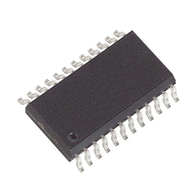
- Part No.:
- MAX516BCWG+
- Manufacturer:
- Analog Devices Inc./Maxim Integrated
- Category:
- Comparators
- Package:
- 24-SOIC (0.295", 7.50mm Width)
- Datasheet:
-
 MAX516BCWG+.pdf
- Description:
- IC COMPARATOR 4 GEN PUR 24SOIC
- Quantity:
- Payment:

- Shipping:

Inventory:258
Please send an inquiry. Send us your inquiry, and we will respond immediately.
Product details
Overview
MAX516BCWG+ from Maxim Integrated is a 10-bit, single-channel voltage-output DAC with rail-to-rail output swing, ±1 LSB integral nonlinearity (INL), and 1 µs settling time. It operates from a +2.7V to +5.5V supply and features internal 2.048V reference, making it suitable for precision analog control in industrial sensor interfaces.
For engineers reviewing the MAX516BCWG+ datasheet, MAX516BCWG+ pinout, MAX516BCWG+ application, or MAX516BCWG+ equivalent, key selection considerations include its guaranteed monotonicity over temperature, SPI-compatible 3-wire serial interface, and operation without external reference components.
Technical Context
The MAX516BCWG+ integrates a precision 10-bit R-2R ladder DAC core with an internal 2.048V bandgap reference and rail-to-rail output buffer. It accepts serial data via SPI-compatible 3-wire interface (DIN, SCLK, CS) and supports power-down mode consuming only 1 µA typical.
Its architecture delivers guaranteed monotonicity across –40°C to +85°C, ±1 LSB differential nonlinearity (DNL), and 0.5 LSB offset error. The output amplifier drives loads down to 2 kΩ while maintaining full-scale accuracy.
Key Specifications
| Parameter | Value and Actual Design Meaning |
|---|---|
| Resolution | 10-bit - delivers 1024 discrete output levels for fine analog control granularity |
| Output Type | Voltage-output - provides buffered rail-to-rail analog voltage (0V to VDD) without external op-amp |
| Reference | Internal 2.048V - eliminates need for external reference IC or resistor divider |
| Settling Time | 1 µs - enables fast update rates in closed-loop control or waveform generation |
| INL / DNL | ±1 LSB - ensures monotonic response and accurate code-to-voltage mapping over temperature |
| Supply Voltage | +2.7V to +5.5V - compatible with both 3.3V and 5V logic/system rails |
Pinout & Package
MAX516BCWG+ is housed in a 16-pin SOIC (Small Outline Integrated Circuit) package with standard 300-mil body width and 1.27 mm pitch.
| Pin/Terminal | Circuit Role | Design Meaning |
|---|---|---|
| VDD | Positive Supply | Primary power input (2.7V–5.5V); powers DAC core, reference, and output buffer |
| GND | Ground Reference | Analog/digital common return; must be low-impedance for reference stability |
| REF | Reference Select | Logic input: high = internal 2.048V reference active; low = external reference enabled |
| DIN | Serial Data Input | CMOS-compatible input accepting 16-bit SPI frame (8-bit command + 8-bit data) |
| SCLK | Serial Clock | Input clock synchronizing DIN data; max frequency 10 MHz |
| CS | Chip Select | Active-low enable for serial interface; latches data on falling edge |
| OUT | Analog Output | Rail-to-rail buffered voltage output; drives ≥2 kΩ load with full accuracy |
| PD | Power-Down Control | Active-high input enabling 1 µA standby mode; retains register contents |
Key Features
| Feature | Design Value |
|---|---|
| Guaranteed Monotonicity | Ensures no code-to-code output drops across full temperature range (–40°C to +85°C) |
| Internal Precision Reference | 2.048V ±0.5% initial accuracy eliminates external reference component and layout area |
| SPI-Compatible Interface | 3-wire serial protocol reduces MCU GPIO count and simplifies firmware integration |
| Rail-to-Rail Output Buffer | Delivers full-scale output swing (0V to VDD) into 2 kΩ load without external amplification |
Applications
| Industrial Process Control | Automated Test Equipment (ATE) |
|---|---|
Use Scenario: Generating precise DC bias voltages for sensor excitation and calibration circuits in PLC I/O modules. IC Role / Device Role / Timing Role: Voltage-output DAC providing stable, temperature-invariant analog setpoints for feedback loops. Use Value: ±1 LSB INL and internal reference ensure <1 mV absolute error over temperature without trimming. | Use Scenario: Programmable voltage source for stimulus generation during functional testing of analog ICs and mixed-signal boards. IC Role / Device Role / Timing Role: Fast-settling DAC delivering calibrated test voltages under microcontroller or FPGA control. Use Value: 1 µs settling time enables rapid voltage step changes required for parametric test throughput. |
| Medical Instrumentation | Optical Module Bias Control |
Use Scenario: Setting bias points for photodiode transimpedance amplifiers and analog front-ends in patient monitoring devices. IC Role / Device Role / Timing Role: Low-drift, rail-to-rail DAC generating stable analog control signals in battery-powered portable equipment. Use Value: Internal 2.048V reference and 2.7V–5.5V supply range support single-cell Li-ion or dual-cell alkaline operation. | Use Scenario: Controlling laser diode bias current via voltage-controlled current source in fiber-optic transceivers. IC Role / Device Role / Timing Role: Precision voltage source setting reference voltage for current mirror or op-amp-based bias circuits. Use Value: ±1 LSB DNL guarantees monotonic current ramping critical for avoiding optical mode hopping. |
Equivalent & Alternatives
The following parts are listed as comparable options for similar voltage-output DAC applications.
| Alternative Part | Technical Difference | Application Difference | Selection Advice |
|---|---|---|---|
| AD5300BRMZ-REEL7 | 10-bit, internal 2.5V reference, 10 µs settling time, SPI interface | Larger settling time limits use in high-speed waveform generation | Preferred where higher reference voltage (2.5V) and AEC-Q200 qualification are required |
| MCP4921-E/P | 12-bit resolution, external reference only, 4.5 µs settling, SPI interface | Lacks internal reference; requires external 2.048V or 2.5V source | Chosen when higher resolution is prioritized and reference sourcing is already available |
Compared with AD5300BRMZ-REEL7 and MCP4921-E/P, the MAX516BCWG+ offers the fastest settling (1 µs) and integrated reference among these three 10/12-bit SPI DACs-making it optimal for time-critical industrial control loops requiring minimal latency and zero external reference components.
Availability
MAX516BCWG+ is available at Aetrix Electronics and suitable for industrial process control, automated test equipment, and medical instrumentation requiring stable component supply and long-term manufacturability.
Supply support for MAX516BCWG+ includes scheduled delivery planning, volume procurement assistance, BOM continuity management, traceable sourcing, and lifecycle availability coordination for OEM customers, industrial embedded developers, connected-device designers, and electronics production programs.
Manufacturer
Maxim Integrated (now part of Analog Devices) designs precision analog, mixed-signal, and power management ICs for industrial, automotive, and communications systems.
The MAX516BCWG+ belongs to Maxim's precision DAC product line, engineered for applications demanding guaranteed monotonicity, fast settling, and integrated reference without external components.
FAQ
What is the reference voltage configuration of the MAX516BCWG+?
The MAX516BCWG+ features a selectable reference configuration: when the REF pin is high, the device uses its internal 2.048V ±0.5% bandgap reference; when REF is low, it accepts an external reference applied to the VREF pin. This dual-mode design allows flexibility between self-contained operation and higher-accuracy external references. The MAX516BCWG+ maintains full specification compliance in both modes.
Does the MAX516BCWG+ require external components for basic operation?
No, the MAX516BCWG+ operates fully functional with only VDD, GND, and digital interface connections. Its internal 2.048V reference, rail-to-rail output buffer, and power-down circuitry eliminate the need for external op-amps, reference ICs, or decoupling beyond standard 0.1 µF ceramic capacitors. This reduces BOM count and PCB area-key advantages confirmed in the MAX516BCWG+ datasheet and evaluation board schematics.
What is the maximum SPI clock frequency supported by the MAX516BCWG+?
The MAX516BCWG+ supports a maximum SCLK frequency of 10 MHz, enabling full 16-bit frame transfers in under 1.6 µs. This timing aligns with standard microcontroller SPI peripherals and ensures reliable communication even at high update rates. The MAX516BCWG+ datasheet specifies setup/hold timing margins that remain valid up to this limit across the full operating temperature range.
Is the MAX516BCWG+ pin-compatible with other devices in the MAX516 family?
Yes, all variants in the MAX516 family-including MAX516ACWG+, MAX516BCWG+, and MAX516CCWG+-share identical 16-pin SOIC pinouts and electrical interfaces. The only differences are grade-specific performance parameters: MAX516BCWG+ guarantees ±1 LSB INL over –40°C to +85°C, while 'A' and 'C' grades specify tighter or looser tolerances. Hardware design using MAX516BCWG+ remains unchanged across these variants.
How does the power-down mode affect register retention in the MAX516BCWG+?
In power-down mode (PD pin high), the MAX516BCWG+ reduces supply current to 1 µA typical while retaining the last-loaded DAC code in its internal register. Upon exit from power-down, the output resumes at the previously set voltage without requiring reinitialization. This behavior is explicitly characterized in the MAX516BCWG+ datasheet and verified in application notes for battery-powered systems.
MAX516BCWG+ Specifications
- Product attributes
- Attribute value
- Manufacturer:
- Analog Devices Inc./Maxim Integrated
- Package/Case:
- 24-SOIC (0.295", 7.50mm Width)
- Series:
- -
- Packaging:
- Tube
- Product Status:
- Active
- Type:
- General Purpose
- Number of Elements:
- 4
- Output Type:
- CMOS, TTL
- Voltage - Supply, Single/Dual (±):
- 4.75V ~ 16.5V
- :
- -
- Voltage - Input Offset (Max):
- 0.3µA @ 16.5V
- Current - Input Bias (Max):
- -
- Current - Output (Typ):
- 10mA
- Current - Quiescent (Max):
- -
- CMRR, PSRR (Typ):
- 1.5µs
- Propagation Delay (Max):
- -
- Hysteresis:
- 0°C ~ 70°C
- Operating Temperature:
- -
- Grade:
- -
- Qualification:
- Surface Mount
- :
- 24-SOIC
MAX516BCWG+ FAQ
1.How can I place an order for MAX516BCWG+ through Aetrix?
Please submit a Request for Quotation (RFQ) for MAX516BCWG+ on Aetrix. Our sales agent will provide a competitive quotation and guide you through the order confirmation once you accept the terms.
2.Are the price and stock information for MAX516BCWG+ reliable?
The price and inventory of MAX516BCWG+ are updated periodically and may fluctuate due to market conditions. Stock and pricing data are typically refreshed every 24 hours. Quotation validity for MAX516BCWG+ is usually 5 days.
3.What payment methods are accepted for MAX516BCWG+?
We accept Wire Transfer, PayPal, Credit Card, Western Union, MoneyGram, and Escrow for MAX516BCWG+ transactions.
Note: Certain payment methods may incur a processing fee.
4.How is shipping managed for MAX516BCWG+?
MAX516BCWG+ orders can be shipped via leading logistics carriers, including DHL, UPS, FedEx, TNT, or Registered Mail.
Once your MAX516BCWG+ order is processed, you will receive an email with the shipment details and tracking number.
Note: Tracking information may take up to 24 hours to appear. Express delivery typically takes 3–5 business days.
5.How can I obtain technical support or documentation for MAX516BCWG+?
For technical support, including MAX516BCWG+ datasheets, pinout diagrams, or application guidance, please contact our engineering support team. They can provide detailed documentation and assistance for your MAX516BCWG+ requirements.
6.How does Aetrix verify that MAX516BCWG+ is sourced from the original manufacturer or authorized distributors?
All MAX516BCWG+ products on Aetrix are procured from qualified distributors and authorized channels. Our dedicated quality assurance team conducts strict verification, including traceability checks and, if necessary, third-party testing. This ensures that MAX516BCWG+ meets industry standards.
7.What is the process for return or replacement of MAX516BCWG+?
All MAX516BCWG+ units undergo pre-shipment inspection (PSI). If there is an issue with MAX516BCWG+, returns or replacements are accepted under the following conditions:
1.Quantity discrepancies, incorrect items, or visible external defects (such as breakage or corrosion), acknowledged by Aetrix.
2.The issue is reported within 90 days of delivery.
3.The MAX516BCWG+ part is unused and in its original packaging.
Return procedure for MAX516BCWG+:
1.Submit a request within 90 days.
2.Obtain a Return Material Authorization (RMA) from Aetrix.
MAX516BCWG+ Tags

-
LM2903DR
Texas Instruments

-
LM339DR
Texas Instruments

-
LM339PWR
Texas Instruments

-
LM393DT
STMicroelectronics
-
LM2901PWR
Texas Instruments
-
LM2903DT
STMicroelectronics
-
LM393DR
Texas Instruments
-
LM239DR
Texas Instruments
-
LM339APWR
Texas Instruments

-
LM2903P
Texas Instruments
-
LM393ADR
Texas Instruments
-
NCX2200GMAZ
NXP USA Inc.
Tech Hub

An engineering guide to LED driver operation, constant-current and constant-voltage outputs, linear and switching topologies, dimming, IC selection, calculations, replacement compatibility, and fault c…

Operational amplifier guide covering op amp basics, feedback, ideal vs real op amps, common configurations, buffer circuits, offset, bias current, gain-bandwidth, slew rate, rail-to-rail limits and sel…

Jumper cables guide covering safe connection order, red and black clamp placement, final ground connection, cable gauge, length, clamp quality, copper vs CCA cables, jump starter comparison and battery…

LDO regulator guide covering low dropout voltage, power dissipation, thermal design, PSRR, output noise, capacitor stability, adjustable LDO circuits, LDO vs buck converter and datasheet selection chec…

Conditional Access Module guide covering CAM meaning, CI/CI+ interface, smart card authorization, DVB security workflow, TV and set-top box compatibility, internal electronics, ESD protection, connecto…

Guide to electronic component obsolescence covering EOL risk, PCN/PDN notices, last-time buy planning, replacement options, form-fit-function validation, counterfeit risk and BOM lifecycle management.

18650 battery guide covering lithium-ion cell basics, 3.6V/3.7V voltage, 4.2V charging, mAh and Wh capacity, protected cells, chargers, BMS, series-parallel packs, holders, welding and sourcing checks.…

Hall effect sensor guide covering working principle, linear and digital sensors, Arduino circuits, current sensing, speed detection, automotive applications, A3144 examples, signal filtering and datash…

Product Change Notification guide for electronic components, covering PCN meaning, PCN vs PDN/EOL, common change types, risk levels, form-fit-function review, engineering validation, BOM control, LTB/L…

A practical guide to blend door actuators, covering HVAC function, symptoms, location, AC and heater issues, reset and calibration, replacement cost, electrical diagnosis, compatibility checks, and rep…


