
 My Inquiry
 My Account


Analog Devices Inc./Maxim Integrated MAX613CPD
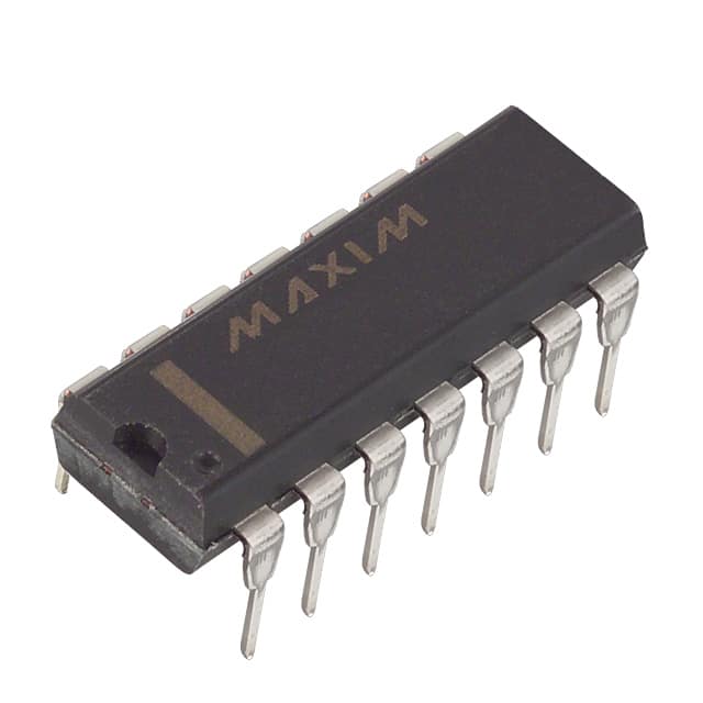
- Part No.:
- MAX613CPD
- Manufacturer:
- Analog Devices Inc./Maxim Integrated
- Package:
- 14-DIP (0.300", 7.62mm)
- Datasheet:
-
 MAX613CPD.pdf
- Description:
- IC PWR CNTRLR ANLG PCMCIA 14-DIP
- Quantity:
- Payment:

- Shipping:

Inventory:1,204
Please send an inquiry. Send us your inquiry, and we will respond immediately.
Product details
Overview
MAX613CPD from Maxim Integrated is a dual-slot PCMCIA analog power controller IC designed to manage VPP supply switching (0V/+5V/+12V/Hi-Z) and level-shifted VCC control for notebook and palmtop memory card slots. It integrates two independent 1.6Ω VPP power switches, open-drain gate drivers (DRV3/DRV5), and logic-compatible inputs for Intel 82365SL and Vadem VG-465 controllers. It operates from 0°C to +70°C in a 14-pin plastic DIP package.
For engineers reviewing the MAX613CPD datasheet, MAX613CPD pinout, MAX613CPD application, or MAX613CPD equivalent, key selection criteria include dual VPP output capability, break-before-make switching integrity, 10mA quiescent current, and compatibility with 3.3V/5V mixed-voltage PCMCIA systems requiring precise VPP1/VPP2 sequencing during flash programming.
Technical Context
The MAX613CPD implements dual independent VPP switching paths using on-chip N-channel power MOSFETs, each controlled by two logic inputs (AVPP1/AVPP0 and BVPP1/BVPP0) to select 0V, VCCIN (+5V), VPPIN (+12V), or high-impedance states. Its internal 1.6Ω switch resistance (12V mode) supports up to 120mA load per channel with minimal voltage drop.
VCC control is handled via open-drain drivers DRV3 and DRV5, whose state is determined by VCC0/VCC1 and SHDN inputs per Table 3; shutdown overrides normal control to force active-low drive. All logic inputs accept standard TTL/CMOS levels (VIH = 2.4V, VIL = 0.8V), ensuring direct interfacing with PCMCIA host controllers without external level translation.
Key Specifications
| Parameter | Value and Actual Design Meaning |
|---|---|
| VPP Switch Resistance (12V mode) | 1.60Ω typical - ensures ≤192mV drop at 120mA, critical for stable flash programming voltage |
| VCCIN Supply Current (5V mode) | 2.25–3.5µA - enables ultra-low standby power in battery-powered palmtop systems |
| VPPIN Supply Current (12V mode) | 0.05–1µA - minimizes auxiliary supply loading during VPP generation |
| Logic Input Voltage Thresholds | VIH = 2.4V, VIL = 0.8V - guarantees reliable operation with Intel 82365SL and Cirrus CL-PD6720 controllers |
| Operating Temperature Range | 0°C to +70°C - validated for commercial-grade notebook and digital camera environments |
| Package Type | 14-pin plastic DIP - provides through-hole mounting for prototyping and legacy industrial designs |
| Break-Before-Make Switching | Hardware-enforced - prevents VPP short-circuit between 0V, +5V, and +12V rails during state transitions |
Pinout & Package
MAX613CPD is housed in a 14-pin plastic DIP (dual in-line package) with 0.3-inch body width and standard through-hole footprint. Pin 1 is marked with a notch or dot; pin numbering follows counter-clockwise convention from top-left corner.
| Pin/Terminal | Circuit Role | Design Meaning |
|---|---|---|
| 1 (VPPIN) | +12V power input | Accepts 0V to +12.6V; powers internal VPP switches and sets upper rail for AVPP/BVPP outputs |
| 2 (GND) | Analog/digital ground reference | Common return for all internal circuitry; must be low-impedance connection to system ground plane |
| 3 (AVPP1) | AVPP state control input | MSB of 2-bit logic code selecting AVPP output: 0V, VCCIN, VPPIN, or Hi-Z (per Table 1) |
| 4 (AVPP0) | AVPP state control input | LSB of 2-bit logic code for AVPP output selection; paired with AVPP1 for full VPP1 control |
| 5 (BVPP1) | BVPP state control input | MSB of 2-bit logic code selecting BVPP output (VPP2); enables independent programming of high/low byte flash banks |
| 6 (BVPP0) | BVPP state control input | LSB of 2-bit logic code for BVPP (VPP2); allows asymmetric VPP1/VPP2 timing to reduce peak +12V current draw |
| 7 (VCC1) | VCC driver enable input | Controls DRV3/DRV5 behavior per Table 3; used with VCC0 to sequence slot VCC power-up/down |
| 8 (VCC0) | VCC driver enable input | Paired with VCC1 to define DRV3/DRV5 output state; supports hot-insertion-safe VCC ramp control |
| 9 (DRV5) | Open-drain VCC gate driver | Sinks current to turn on external N-channel MOSFET for Slot B VCC; requires external pull-up (e.g., to VPPIN) |
| 10 (DRV3) | Open-drain VCC gate driver | Sinks current to turn on external N-channel MOSFET for Slot A VCC; rise time set by external pull-up resistor |
| 11 (SHDN) | Global shutdown input | Active-low override: forces DRV3/DRV5 low regardless of VCC0/VCC1 when pulled to GND |
| 12 (BVPP) | Switched VPP2 output | Delivers selected voltage (0V/VCCIN/VPPIN/Hi-Z) to PCMCIA Slot B VPP2 pin; bypass capacitor ≥0.01µF required |
| 13 (AVPP) | Switched VPP1 output | Delivers selected voltage to PCMCIA Slot A VPP1 pin; supports separate erase/program cycles for low/high byte flash banks |
| 14 (VCCIN) | +5V logic supply input | Powers internal logic and gate drivers; must be ≥2.85V for proper DRV3/DRV5 operation; independent of VPPIN |
Key Features
| Feature | Design Value |
|---|---|
| Dual independent VPP switching | Separate AVPP (VPP1) and BVPP (VPP2) outputs enable byte-level flash programming to halve +12V peak current demand |
| 1.6Ω internal VPP switches | Minimizes IR drop under 120mA load, maintaining ≥11.8V at AVPP/BVPP during flash erase cycles |
| Break-before-make logic | Hardware-guaranteed dead-time between VPP state transitions prevents rail-to-rail short circuits during voltage changes |
| Open-drain VCC drivers (DRV3/DRV5) | Enable controlled, slow-ramp VCC power delivery via external pull-up resistors-critical for hot-insertion compliance |
| PCMCIA controller compatibility | Direct interface with Intel 82365SL, Vadem VG-465/468, and Cirrus CL-PD6710/6720 without level-shifting components |
Applications
| Flash Memory Programming | Notebook PCMCIA Slots |
|---|---|
|
Use Scenario: Simultaneous erase/program of 16-bit flash memory cards where low-order and high-order bytes require separate VPP control. IC Role / Device Role / Timing Role: MAX613CPD acts as dual-rail VPP sequencer, delivering independent 0V/+5V/+12V to VPP1 and VPP2 pins while enforcing break-before-make timing. Use Value: Enables 30mA-per-byte flash programming instead of 60mA simultaneous draw, allowing use of low-power +12V charge pumps like MAX662. |
Use Scenario: Power management in dual-slot notebook PCs supporting both Type I and Type II PCMCIA cards. IC Role / Device Role / Timing Role: MAX613CPD serves as analog power hub-switching VPP for memory cards and controlling VCC via DRV3/DRV5 to prevent hot-insertion damage. Use Value: Eliminates need for discrete MOSFETs and level shifters, reducing BOM count and PCB area in space-constrained laptop designs. |
| Digital Camera Storage | Handheld Terminal Expansion |
|
Use Scenario: Compact digital cameras using PCMCIA-based CompactFlash adapters for removable storage. IC Role / Device Role / Timing Role: MAX613CPD manages VPP during firmware updates and image buffer writes, with VCC sequencing ensuring safe card insertion/removal. Use Value: Supports 0°C to +70°C operation and <10µA total quiescent current-extending battery life during standby with CF card inserted. |
Use Scenario: Industrial handheld terminals with PCMCIA slots for barcode scanner or RFID modules. IC Role / Device Role / Timing Role: MAX613CPD provides robust VPP switching and VCC control across temperature extremes, interfacing directly with Vadem VG-465 controller. Use Value: Guarantees reliable flash programming even with noisy 12V supplies, thanks to internal 1.6Ω switches and dedicated VPPIN bypassing requirements. |
Equivalent & Alternatives
The following parts are listed as comparable options for similar dual-slot PCMCIA analog power control applications.
| Alternative Part | Technical Difference | Application Difference | Selection Advice |
|---|---|---|---|
| MAX613CSD | Same electrical specs and pinout, but in 14-pin SO package (surface-mount) | Required for automated SMT assembly; lacks through-hole mounting for manual prototyping | Select MAX613CSD for volume production PCBs with reflow soldering; MAX613CPD preferred for breadboarding and repair. |
| MAX614CPA | Single-VPP version (8-pin DIP); no BVPP or DRV3 pins; reduced feature set | Suitable only for single-slot systems; cannot support independent VPP1/VPP2 sequencing | Choose MAX614CPA only when designing for single-slot devices like palmtop organizers-no VPP1/VPP2 coordination needed. |
Compared with MAX613CSD and MAX614CPA, the MAX613CPD uniquely delivers dual independent VPP control in a through-hole package, enabling both rapid prototyping and byte-level flash programming in commercial-temperature notebook and camera platforms without layout redesign.
Availability
MAX613CPD is available at Aetrix Electronics and suitable for notebook computers, digital cameras, and handheld terminals requiring stable component supply with commercial-temperature reliability and through-hole manufacturability.
Supply support for MAX613CPD includes scheduled delivery planning, volume procurement assistance, BOM continuity management, traceable sourcing, and lifecycle availability coordination for OEM customers, industrial embedded developers, connected-device designers, and electronics production programs.
Manufacturer
Maxim Integrated (now part of Analog Devices) is a U.S.-based semiconductor company specializing in precision analog, mixed-signal, and power management ICs for computing, communications, and industrial applications.
The MAX613CPD belongs to Maxim's PCMCIA power controller product line, engineered specifically to simplify analog power sequencing in portable computing devices with legacy PCMCIA interfaces and stringent low-power requirements.
FAQ
What is the maximum load current supported by each VPP output of the MAX613CPD?
The MAX613CPD supports up to 120mA per VPP output (AVPP or BVPP) in 12V mode with ≤1.6Ω on-resistance, ensuring ≤192mV voltage drop. This rating is validated per Typical Operating Characteristics curves at +25°C and confirmed across the full 0°C to +70°C operating range, making MAX613CPD suitable for driving multiple 8-bit flash chips simultaneously in notebook PCMCIA slots.
Does the MAX613CPD require external MOSFETs for VCC switching, and if so, what type is recommended?
Yes, the MAX613CPD requires external N-channel power MOSFETs for VCC switching-its DRV3 and DRV5 pins are open-drain gate drivers. Recommended devices include the Siliconix Si9956DY or Motorola MTP3055EL: logic-level types with RDS(on) <50mΩ at VGS = 4.5V, enabling full enhancement with pull-up voltages as low as +10V. The MAX613CPD datasheet specifies that gate drive must exceed VCC by ≥4.5V for reliable turn-on, which the MAX613CPD itself does not generate.
Can the MAX613CPD operate with a 3.3V VCCIN supply, or is +5V mandatory?
The MAX613CPD requires VCCIN between 2.85V and 5.5V, but its logic thresholds and driver performance are specified at VCCIN = +5V. While 3.3V operation is electrically possible per Absolute Maximum Ratings, the MAX613CPD's DRV3/DRV5 gate drivers may not sink sufficient current below 4.5V, and VPP switch resistance increases significantly below 4.5V. For guaranteed 3.3V/5V mixed-slot systems, the MAX613CPD must be powered from +5V, with external level shifting applied only to controller signals-not VCCIN.
How does the SHDN pin affect the MAX613CPD's VPP outputs and gate drivers?
The SHDN pin on the MAX613CPD is an active-low global shutdown input that overrides all logic controls: when SHDN = 0V, DRV3 and DRV5 are forced low (sinking current), regardless of VCC0/VCC1 states, ensuring immediate VCC discharge. However, SHDN has no effect on AVPP or BVPP outputs-their states remain determined solely by AVPP1/AVPP0 and BVPP1/BVPP0. This separation allows independent VPP hold while forcing VCC shutdown during hot-removal sequences.
Is the MAX613CPD pin-compatible with newer Maxim PCMCIA controllers like the MAX1601 or MAX1602?
No, the MAX613CPD is not pin-compatible with MAX1601 or MAX1602. Those are later-generation, single-chip PCMCIA power managers integrating VPP generation, VCC regulation, and hot-swap protection in QFN packages-unlike the MAX613CPD's discrete VPP switching and external VCC MOSFET architecture. The MAX613CPD's 14-pin DIP layout, pin functions (e.g., separate AVPP1/BVPP1 inputs), and lack of integrated regulators make it incompatible with MAX1601/MAX1602 footprints or signal routing.
MAX613CPD Specifications
- Product attributes
- Attribute value
- Manufacturer:
- Analog Devices Inc./Maxim Integrated
- Package/Case:
- 14-DIP (0.300", 7.62mm)
- Series:
- -
- Packaging:
- Tube
- Product Status:
- Obsolete
- Switch Type:
- PCMCIA Switch
- Number of Outputs:
- 2
- Ratio - Input:Output:
- -
- Output Configuration:
- -
- Output Type:
- -
- Interface:
- -
- Voltage - Load:
- -
- Voltage - Supply (Vcc/Vdd):
- -
- Current - Output (Max):
- -
- Rds On (Typ):
- -
- Input Type:
- -
- Features:
- -
- Fault Protection:
- -
- Operating Temperature:
- 0°C ~ 70°C
- Grade:
- -
- Qualification:
- -
- Mounting Type:
- Through Hole
- Supplier Device Package:
- 14-PDIP
MAX613CPD FAQ
1.How can I place an order for MAX613CPD through Aetrix?
Please submit a Request for Quotation (RFQ) for MAX613CPD on Aetrix. Our sales agent will provide a competitive quotation and guide you through the order confirmation once you accept the terms.
2.Are the price and stock information for MAX613CPD reliable?
The price and inventory of MAX613CPD are updated periodically and may fluctuate due to market conditions. Stock and pricing data are typically refreshed every 24 hours. Quotation validity for MAX613CPD is usually 5 days.
3.What payment methods are accepted for MAX613CPD?
We accept Wire Transfer, PayPal, Credit Card, Western Union, MoneyGram, and Escrow for MAX613CPD transactions.
Note: Certain payment methods may incur a processing fee.
4.How is shipping managed for MAX613CPD?
MAX613CPD orders can be shipped via leading logistics carriers, including DHL, UPS, FedEx, TNT, or Registered Mail.
Once your MAX613CPD order is processed, you will receive an email with the shipment details and tracking number.
Note: Tracking information may take up to 24 hours to appear. Express delivery typically takes 3–5 business days.
5.How can I obtain technical support or documentation for MAX613CPD?
For technical support, including MAX613CPD datasheets, pinout diagrams, or application guidance, please contact our engineering support team. They can provide detailed documentation and assistance for your MAX613CPD requirements.
6.How does Aetrix verify that MAX613CPD is sourced from the original manufacturer or authorized distributors?
All MAX613CPD products on Aetrix are procured from qualified distributors and authorized channels. Our dedicated quality assurance team conducts strict verification, including traceability checks and, if necessary, third-party testing. This ensures that MAX613CPD meets industry standards.
7.What is the process for return or replacement of MAX613CPD?
All MAX613CPD units undergo pre-shipment inspection (PSI). If there is an issue with MAX613CPD, returns or replacements are accepted under the following conditions:
1.Quantity discrepancies, incorrect items, or visible external defects (such as breakage or corrosion), acknowledged by Aetrix.
2.The issue is reported within 90 days of delivery.
3.The MAX613CPD part is unused and in its original packaging.
Return procedure for MAX613CPD:
1.Submit a request within 90 days.
2.Obtain a Return Material Authorization (RMA) from Aetrix.
MAX613CPD Tags

-
TPS22919DCKR
Texas Instruments

-
MIC2091-1YM5-TR
Microchip Technology

-
MIC2090-1YM5-TR
Microchip Technology

-
TPS22995RZFR
Texas Instruments

-
TPS22975DSGR
Texas Instruments

-
SIP32510DT-T1-GE3
Vishay Siliconix

-
ULN2003D1013TR
STMicroelectronics

-
MIC2005A-1YM5-TR
Microchip Technology

-
MIC2005A-1YM6-TR
Microchip Technology

-
TPS22916BYFPR
Texas Instruments

-
TPS22917DBVR
Texas Instruments

-
ULN2003APWR
Texas Instruments
Tech Hub

A practical engineering guide to 3.3V and 5V logic compatibility, input thresholds, resistor dividers, translator ICs, MOSFET level shifting, I2C pull-ups, timing limits and power-sequencing risks.

The 74HC595 uses push-pull logic outputs, while the TPIC6B595 uses 50 V open-drain DMOS sinks for higher-power loads. This guide compares timing, current limits, 3.3 V interfacing, load wiring, thermal…

The 74HC595 converts serial data into eight stable parallel outputs. This guide covers pin functions, shift and storage timing, OE and MR behavior, drive-current limits, cascading, voltage compatibilit…

A technical comparison of level-sensitive latches and edge-triggered flip-flops, covering timing windows, setup and hold limits, master–slave operation, time borrowing, race-through, HDL inference and…

A D latch stores one bit while Enable controls when data can pass. This reference covers gate-level operation, truth tables, transparency, setup and hold timing, LE versus OE, common ICs and practical …

An SR latch stores one bit through cross-coupled feedback. This engineering reference covers NOR and NAND implementations, truth tables, forbidden-state recovery, gated operation, switch debouncing, fa…

Latch circuits retain one bit through feedback. This technical reference covers SR and D latches, truth tables, transparency, timing limits, latch-versus-flip-flop behavior, applications and common log…

An engineering guide to LED driver operation, constant-current and constant-voltage outputs, linear and switching topologies, dimming, IC selection, calculations, replacement compatibility, and fault c…

Operational amplifier guide covering op amp basics, feedback, ideal vs real op amps, common configurations, buffer circuits, offset, bias current, gain-bandwidth, slew rate, rail-to-rail limits and sel…

Jumper cables guide covering safe connection order, red and black clamp placement, final ground connection, cable gauge, length, clamp quality, copper vs CCA cables, jump starter comparison and battery…


