Send an Inquiry

To receive a quote for your project, please fill in the following information, and we’ll get back to you promptly.

Name*
Company*
Email Address*
Phone/WhatsApp
Part Number*
Quantity*
Message
Submit Inventory List

Please fill in the following information, and we’ll get back to you promptly.

Name*
Company*
Email Address*
Phone/WhatsApp
Upload My List
Message

Analog Devices Inc./Maxim Integrated MAX6470TA30BD3
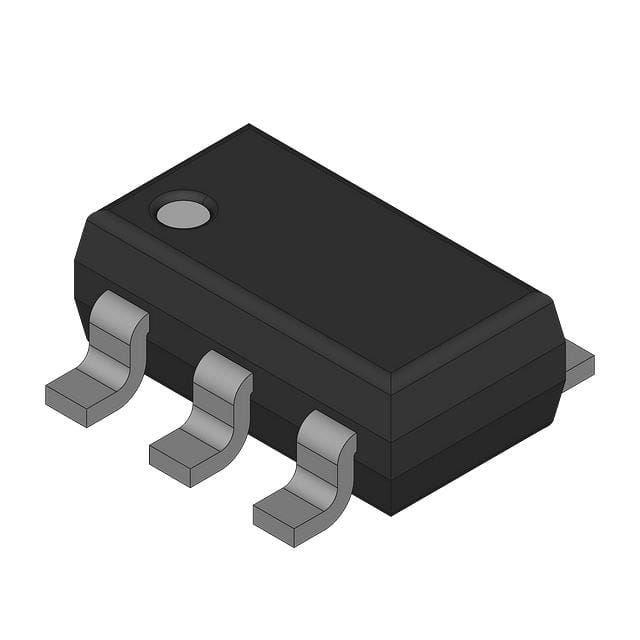
Part No.:
MAX6470TA30BD3
Manufacturer:
Analog Devices Inc./Maxim Integrated
Category:
Voltage Regulators - Linear, Low Drop Out (LDO) Regulators
Package:
8-WDFN Exposed Pad
Datasheet:
AetrixMAX6470TA30BD3.pdf
Description:
IC REG LINEAR LDO 300MA
Quantity:
Payment:
Payment
Shipping:
Shipping

Inventory:1,292

Please send an inquiry. Send us your inquiry, and we will respond immediately.

Part Number
Quantity*
Price
Name*
Company
Email*
Comments

Product details

Overview

MAX6470TA30BD3 from Maxim Integrated is a 3.0V fixed-output, 300mA low-dropout linear regulator with integrated microprocessor reset circuit, 82µA quiescent current, and 150ms minimum reset timeout. It features active-low push-pull RESET, shutdown control (0.1µA standby), and ±2.0% output voltage accuracy over -40°C to +85°C - designed for battery-powered portable systems requiring reliable power sequencing and brownout protection.

For engineers reviewing the MAX6470TA30BD3 datasheet, MAX6470TA30BD3 pinout, MAX6470TA30BD3 application, or MAX6470TA30BD3 equivalent, this device delivers verified LDO regulation with built-in reset supervision, eliminating external supervisors in space-constrained handheld instruments, USB peripherals, and Bluetooth modules where stable 3.0V rail integrity and deterministic power-up timing are critical.

Technical Context

The MAX6470TA30BD3 implements a single-stage PMOS pass transistor architecture with internal bandgap reference and precision comparator-based reset monitoring. Its reset circuit uses the same reference as the regulator core, ensuring correlated tolerance tracking between VOUT and reset threshold (–7.5% or –12.5% of nominal output).

This variant is configured for 3.0V fixed output (suffix "30"), 12.5% reset threshold accuracy (suffix "B"), and 150ms minimum reset timeout (suffix "D3"). It includes active-low SHDN input and push-pull RESET output - no manual reset (MR) or remote sense (FB) functionality, distinguishing it from MAX6471–MAX6474 and MAX6475–MAX6476 variants.

Key Specifications

Parameter Value and Actual Design Meaning
Output Voltage Fixed 3.0V ±2.0% over –40°C to +85°C - ensures stable logic-level supply for 3.3V-tolerant microcontrollers without external feedback.
Max Output Current 300mA guaranteed - supports moderate-power digital loads like baseband processors or RF transceivers in portable devices.
Dropout Voltage 114mV at 300mA load - enables operation down to VIN = 3.114V, extending battery runtime in single-cell Li-ion or 3× alkaline systems.
Quiescent Current 82µA typical - minimizes standby drain in always-on subsystems such as real-time clocks or sensor wake logic.
Reset Timeout 150ms minimum - provides sufficient hold-off for oscillator stabilization and firmware initialization before processor release.
Reset Threshold –12.5% of VOUT (2.625V) - asserts RESET when regulated 3.0V rail drops below 2.625V, meeting standard µP supply tolerance requirements.
Shutdown Current 0.1µA typical - enables deep-sleep mode with near-zero leakage during system hibernation.

Pinout & Package

MAX6470TA30BD3 is housed in an 8-pin TDFN-EP (3mm × 3mm, 0.5mm pitch) package with exposed thermal pad. Pin 1 is IN; Pin 2 is GND; Pin 3 is SHDN; Pin 4 is RESET; Pin 5 is SET; Pin 6 is OUT; Pins 7–8 are NC; EP is internally connected to GND and must be soldered to PCB ground plane for thermal management.

Pin/Terminal Circuit Role Design Meaning
IN Regulator input Accepts 2.5V–5.5V input; bypass with 0.1µF ceramic capacitor to GND for stability.
GND Power and thermal ground Primary return path; also serves as heatsink - requires direct connection to large copper area.
SHDN Active-low shutdown control Pull low to disable regulator and reduce supply current to 0.1µA; tie to IN for normal operation.
RESET Active-low push-pull reset output Drives µP reset pin directly; remains low for ≥150ms after VOUT rises above 2.625V.
SET Feedback configuration input Connected to GND to select fixed 3.0V output; left unconnected or pulled to GND - not used for adjustment in this variant.
OUT Regulated output Delivers up to 300mA at 3.0V; requires ≥3.3µF low-ESR ceramic output capacitor.

Key Features

Feature Design Value
Integrated reset supervisor Eliminates need for discrete supervisor IC - reduces BOM count and board area in compact portable designs.
Low dropout voltage 114mV at full 300mA load enables >95% efficiency at 3.0V output from 3.3V input rails.
Ultra-low quiescent current 82µA operation + 0.1µA shutdown supports multi-year battery life in IoT edge sensors and wearables.
Thermal and short-circuit protection Auto-recovery thermal shutdown at +180°C and 450mA current limit prevent damage during fault conditions.
Reverse current blocking 0.01µA typical OUT-to-IN leakage prevents backfeed into depleted batteries during hot-swap or backup scenarios.

Applications

Handheld Instruments USB Peripheral Devices

Use Scenario: Powering ARM Cortex-M based data loggers in field-deployed PDAs with single-cell Li-ion battery.

IC Role / Device Role / Timing Role: Primary 3.0V LDO regulator and power-on reset generator - ensures µP starts only after stable 3.0V rail and clock stabilization.

Use Value: 150ms reset timeout guarantees bootloader execution completes before peripheral enumeration begins, preventing USB descriptor failures.

Use Scenario: Regulating 3.0V supply for USB-to-UART bridge ICs in compact dongles powered from host USB VBUS.

IC Role / Device Role / Timing Role: Input-conditioned LDO with brownout detection - maintains clean 3.0V rail during USB port hot-plug transients.

Use Value: 82µA quiescent current minimizes parasitic draw when host suspends bus power, extending suspend duration.

Bluetooth Audio Modules Notebook Subsystem Rails

Use Scenario: Supplying 3.0V to BLE SoC and audio codec in wireless earbud charging case electronics.

IC Role / Device Role / Timing Role: Low-noise, low-IQ power source with integrated reset - coordinates power-up sequence between RF and DSP blocks.

Use Value: Push-pull RESET eliminates need for external pull-up resistor, reducing component count and layout complexity in 3×3mm footprint.

Use Scenario: Generating auxiliary 3.0V rail for embedded controller (EC) or keyboard backlight driver in ultrabook platforms.

IC Role / Device Role / Timing Role: Secondary regulated supply with independent reset assertion - isolates EC boot timing from main CPU VRM behavior.

Use Value: ±2.0% output accuracy ensures EC operates within spec across temperature, avoiding false watchdog timeouts.

Equivalent & Alternatives

The following parts are listed as comparable options for similar LDO-with-reset applications.

Alternative Part Technical Difference Application Difference Selection Advice
TPS76330DBVR 300mA LDO with 120ms reset timeout, no shutdown pin, open-drain RESET only Lacks SHDN control and push-pull RESET - requires external pull-up and cannot enter ultra-low-power state Select when board already includes pull-up and shutdown is unnecessary; verify reset timing compatibility with µP requirements
NCP1117ST30T3G 800mA LDO with no integrated reset - requires external supervisor (e.g., MCP102) Higher current capability but increases BOM cost and layout area; no built-in power sequencing Choose only if >300mA load demand exists and discrete reset supervision is acceptable for design constraints

Compared with TPS76330DBVR and NCP1117ST30T3G, MAX6470TA30BD3 uniquely integrates push-pull RESET, active-low SHDN, and 150ms timeout in a single 3×3mm TDFN package - delivering lower system-level component count and tighter power-up coordination for portable 3.0V applications.

Availability

MAX6470TA30BD3 is available at Aetrix Electronics and suitable for handheld instruments, USB peripheral devices, and Bluetooth modules requiring stable component supply with guaranteed long-term manufacturability and RoHS-compliant packaging.

Supply support for MAX6470TA30BD3 includes scheduled delivery planning, volume procurement assistance, BOM continuity management, traceable sourcing, and lifecycle availability coordination for OEM customers, industrial embedded developers, connected-device designers, and electronics production programs.

Manufacturer

Maxim Integrated (now part of Analog Devices) is a semiconductor company specializing in high-performance analog, mixed-signal, and power management solutions for industrial, communications, and consumer applications.

MAX6470TA30BD3 belongs to the MAX6469–MAX6484 family of ultra-low-IQ LDOs with integrated reset - engineered specifically for battery-powered portable equipment where minimal standby current, precise reset timing, and small footprint are mandatory.

FAQ

What is the exact output voltage tolerance of the MAX6470TA30BD3 over temperature?

The MAX6470TA30BD3 guarantees ±2.0% output voltage accuracy over the full –40°C to +85°C operating range. This specification applies to fixed-output operation with SET tied to GND, and is measured at load currents from 1mA to 300mA. At +25°C and 1mA ≤ IOUT ≤ 150mA, the tighter ±1.3% tolerance applies - confirmed in the Electrical Characteristics table under "Output Voltage Accuracy (Fixed Output Voltage Operation)".

Does the MAX6470TA30BD3 support adjustable output voltage?

No, the MAX6470TA30BD3 is factory-configured for fixed 3.0V output. Its SET pin is internally connected to the feedback network and must be tied to GND to enable the preset voltage - it does not support external resistor-divider adjustment. Adjustable variants (e.g., MAX6470UT30BD3) use SOT23-6 packaging and different internal routing; this TDFN variant lacks that capability per the Functional Diagram and Pin Description sections.

What is the function of the SHDN pin on the MAX6470TA30BD3?

The SHDN pin on the MAX6470TA30BD3 is an active-low digital control input that disables the regulator core when pulled low, reducing total supply current to 0.1µA (typ). During shutdown, the pass transistor, reference, and control circuitry are powered down. For normal operation, SHDN must be tied to IN (not left floating), as specified in the Pin Description and Absolute Maximum Ratings tables.

Can the MAX6470TA30BD3 be used with a 2.5V input supply?

Yes, the MAX6470TA30BD3 supports input voltages from 2.5V to 5.5V. With a 2.5V input and 3.0V output requirement, the device operates in dropout - its 114mV dropout voltage at 300mA means it cannot regulate 3.0V from 2.5V. Minimum viable input is 3.114V (3.0V + 114mV) at full load. At lighter loads, dropout decreases (e.g., 55mV at 150mA), enabling marginal operation down to ~3.055V.

Is the RESET output of the MAX6470TA30BD3 push-pull or open-drain?

The MAX6470TA30BD3 features a push-pull active-low RESET output, as indicated by the "A" suffix in the ordering guide (MAX6470TAxxx = push-pull; MAX6470TBxxx = open-drain). This allows direct drive of microprocessor reset inputs without external pull-up resistors - confirmed in the Pin Description (Pin 4: RESET - "push-pull configurations") and Electrical Characteristics (RESET Output Voltage VOH/VOL specs).

MAX6470TA30BD3 Specifications

Product attributes
Attribute value
Manufacturer:
Analog Devices Inc./Maxim Integrated
Series:
-
Package/Case:
8-WDFN Exposed Pad
Packaging:
Bulk
Product Status:
Active
Output Configuration:
Positive
Output Type:
Adjustable (Fixed)
Number of Regulators:
1
Voltage - Input (Max):
5.5V
Voltage - Output (Min/Fixed):
1.2V (2.8V)
Voltage - Output (Max):
5.5V
Voltage Dropout (Max):
0.21V @ 300mA
Current - Output:
300mA
Current - Quiescent (Iq):
136 µA
Current - Supply (Max):
96 µA
PSRR:
-
Control Features:
Reset, Shutdown
Protection Features:
Over Current, Over Temperature, Reverse Polarity, Short Circuit
Operating Temperature:
-40°C ~ 85°C (TA)
Grade:
-
Qualification:
-
Mounting Type:
Surface Mount
Supplier Device Package:
8-TDFN (3x3)

MAX6470TA30BD3 FAQ

1.How can I place an order for MAX6470TA30BD3 through Aetrix?

Please submit a Request for Quotation (RFQ) for MAX6470TA30BD3 on Aetrix. Our sales agent will provide a competitive quotation and guide you through the order confirmation once you accept the terms.

2.Are the price and stock information for MAX6470TA30BD3 reliable?

The price and inventory of MAX6470TA30BD3 are updated periodically and may fluctuate due to market conditions. Stock and pricing data are typically refreshed every 24 hours. Quotation validity for MAX6470TA30BD3 is usually 5 days.

3.What payment methods are accepted for MAX6470TA30BD3?

We accept Wire Transfer, PayPal, Credit Card, Western Union, MoneyGram, and Escrow for MAX6470TA30BD3 transactions.

Note: Certain payment methods may incur a processing fee.

4.How is shipping managed for MAX6470TA30BD3?

MAX6470TA30BD3 orders can be shipped via leading logistics carriers, including DHL, UPS, FedEx, TNT, or Registered Mail.

Once your MAX6470TA30BD3 order is processed, you will receive an email with the shipment details and tracking number.

Note: Tracking information may take up to 24 hours to appear. Express delivery typically takes 3–5 business days.

5.How can I obtain technical support or documentation for MAX6470TA30BD3?

For technical support, including MAX6470TA30BD3 datasheets, pinout diagrams, or application guidance, please contact our engineering support team. They can provide detailed documentation and assistance for your MAX6470TA30BD3 requirements.

6.How does Aetrix verify that MAX6470TA30BD3 is sourced from the original manufacturer or authorized distributors?

All MAX6470TA30BD3 products on Aetrix are procured from qualified distributors and authorized channels. Our dedicated quality assurance team conducts strict verification, including traceability checks and, if necessary, third-party testing. This ensures that MAX6470TA30BD3 meets industry standards.

7.What is the process for return or replacement of MAX6470TA30BD3?

All MAX6470TA30BD3 units undergo pre-shipment inspection (PSI). If there is an issue with MAX6470TA30BD3, returns or replacements are accepted under the following conditions:

1.Quantity discrepancies, incorrect items, or visible external defects (such as breakage or corrosion), acknowledged by Aetrix.

2.The issue is reported within 90 days of delivery.

3.The MAX6470TA30BD3 part is unused and in its original packaging.

Return procedure for MAX6470TA30BD3:

1.Submit a request within 90 days.

2.Obtain a Return Material Authorization (RMA) from Aetrix.

MAX6470TA30BD3 Tags

  • MAX6470TA30BD3
  • MAX6470TA30BD3 PDF
  • MAX6470TA30BD3 Datasheet
  • MAX6470TA30BD3 Specifications
  • MAX6470TA30BD3 Images
  • Analog Devices Inc./Maxim Integrated
  • Analog Devices Inc./Maxim Integrated MAX6470TA30BD3
  • Buy MAX6470TA30BD3
  • MAX6470TA30BD3 Price
  • MAX6470TA30BD3 Distributor
  • MAX6470TA30BD3 Supplier
  • MAX6470TA30BD3 Wholesale
Related Products
MIC5504-1.8YM5-TR
MIC5504-1.8YM5-TR

Microchip Technology

MIC5504-3.3YM5-TR
MIC5504-3.3YM5-TR

Microchip Technology

MIC5365-3.0YC5-TR
MIC5365-3.0YC5-TR

Microchip Technology

MIC5365-1.8YC5-TR
MIC5365-1.8YC5-TR

Microchip Technology

MIC5365-2.5YC5-TR
MIC5365-2.5YC5-TR

Microchip Technology

MIC5365-3.3YC5-TR
MIC5365-3.3YC5-TR

Microchip Technology

MIC5365-3.3YD5-TR
MIC5365-3.3YD5-TR

Microchip Technology

MIC5317-3.3YM5-TR
MIC5317-3.3YM5-TR

Microchip Technology

TLV1117LV33DCYR
TLV1117LV33DCYR

Texas Instruments

MIC5317-3.3YMT-TZ
MIC5317-3.3YMT-TZ

Microchip Technology

MIC5528-3.3YMT-TR
MIC5528-3.3YMT-TR

Microchip Technology

TLV75801PDRVR
TLV75801PDRVR

Texas Instruments

Tech Hub

Search

Search

PRODUCT

PRODUCT

PHONE

PHONE

USER

USER












