
 My Inquiry
 My Account


Analog Devices Inc./Maxim Integrated MAX6604ATA+
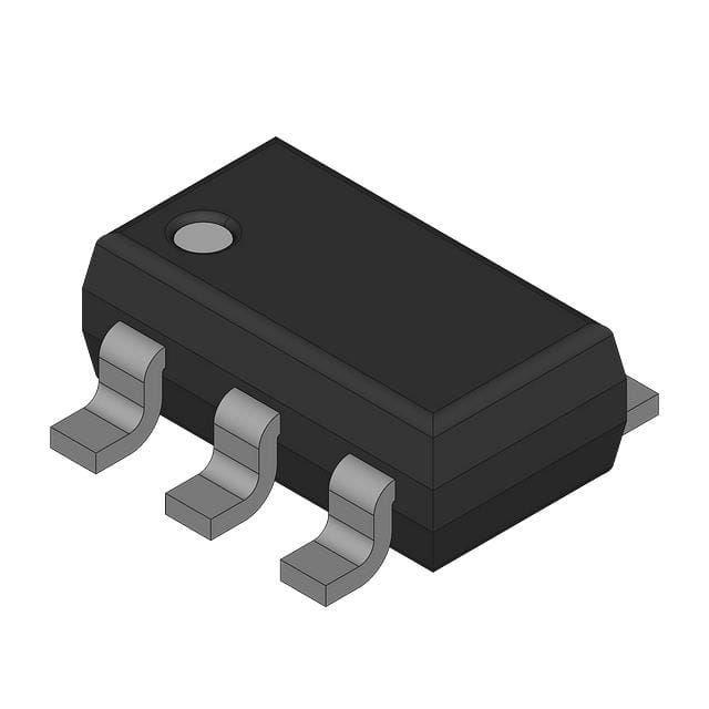
- Part No.:
- MAX6604ATA+
- Manufacturer:
- Analog Devices Inc./Maxim Integrated
- Category:
- Thermal Management
- Package:
- 8-WFDFN Exposed Pad
- Datasheet:
-
 MAX6604ATA+.pdf
- Description:
- PRECISION TEMPERATURE MONITOR
- Quantity:
- Payment:

- Shipping:

Inventory:2,202
Please send an inquiry. Send us your inquiry, and we will respond immediately.
Product details
Overview
MAX6604ATA+ from Maxim Integrated is a high-precision SMBus/I²C-compatible temperature sensor designed specifically for thermal monitoring on DDR memory modules. It delivers ±1°C accuracy over –20°C to +125°C, updates temperature data 8 times per second, and features programmable overtemperature interrupt thresholds via its digital interface. Its placement directly on the memory module enables accurate, responsive thermal tracking critical for DDR thermal management.
For engineers reviewing the MAX6604ATA+ datasheet, MAX6604ATA+ pinout, MAX6604ATA+ application, or MAX6604ATA+ equivalent, key selection considerations include its 8-pin TDFN (2mm × 3mm) package, ±1°C measurement accuracy across full operating range, 8 Hz conversion rate, and support for up to eight devices on one SMBus with A0–A2 address inputs.
Technical Context
The MAX6604ATA+ functions as an SMBus/I²C slave device with a fixed 7-bit base address (0011xxx0) configurable via three hardware address pins (A0–A2), enabling up to eight sensors on a single bus. It implements a 16-bit register map including read-only temperature data (0.125°C LSB), programmable alarm/critical trip thresholds (0.25°C LSB), and configuration control for EVENT output mode (interrupt/comparator/critical-only) and polarity.
Its thermal sensing core continuously samples die temperature and latches results at 8 Hz; conversion time is 125 ms. The EVENT pin operates as an open-drain output supporting three distinct functional modes-each defined by bits in the Configuration Register (address 01h)-and responds to crossing of user-defined upper/lower alarm or critical thresholds, with optional hysteresis (1.5°C/3°C/6°C).
Key Specifications
| Parameter | Value and Actual Design Meaning |
|---|---|
| Temperature Accuracy | ±1°C from –20°C to +125°C - ensures reliable DDR module thermal margining without motherboard sensor lag or spatial error |
| Conversion Rate | 8 Hz - provides real-time thermal response suitable for dynamic DDR power-state transitions |
| Supply Voltage Range | +2.7 V to +3.6 V - compatible with standard DDR module VDDQ rails and eliminates need for external LDO |
| Operating Current | 300 µA typical - minimizes loading on memory module power delivery network |
| Shutdown Current | 3 µA typical - enables low-power thermal monitoring during system suspend states |
| Interface Protocol | SMBus/I²C-compatible, 100 kHz max clock - interoperable with standard platform controller hub (PCH) thermal management firmware |
| Address Inputs | A0, A1, A2 - allow hardware-selectable slave address for multi-module configurations without software reconfiguration |
Pinout & Package
MAX6604ATA+ is housed in an 8-pin TDFN-EP package (2mm × 3mm, 0.75mm height) with exposed pad (EP) internally connected to GND. The EP must be soldered to a large PCB ground plane for optimal thermal and electrical performance.
| Pin/Terminal | Circuit Role | Design Meaning |
|---|---|---|
| A0 | Address Input | Hardwired to GND or VCC to set LSB of 7-bit SMBus slave address (0011-A2-A1-A0-0) |
| A1 | Address Input | Hardwired to GND or VCC to set middle bit of SMBus slave address |
| A2 | Address Input | Hardwired to GND or VCC to set MSB of SMBus slave address - enables up to eight devices on one bus |
| GND | Ground Reference | Primary analog/digital return; EP pad is internally tied to this node |
| SDA | Serial Data I/O | Open-drain bidirectional bus line requiring external pullup; carries command/data bytes and ACK/NACK |
| SCL | Serial Clock Input | Input-only clock line synchronized to SMBus timing; defines data sampling edges |
| EVENT | Interrupt Output | Open-drain active-low (default) output signaling alarm/critical threshold crossing; configurable via register |
| VCC | Power Supply | +2.7 V to +3.6 V input; requires local 0.1 µF ceramic bypass capacitor placed adjacent to pin |
Key Features
| Feature | Design Value |
|---|---|
| JEDEC-compliant DDR thermal monitoring | Fully aligned with JEDEC specifications for memory module temperature sensing - validated for use in DDR2/DDR3 DIMMs and SO-DIMMs |
| Programmable overtemperature interrupt | Independent upper/lower alarm and critical trip thresholds stored in dedicated 16-bit registers (02h–04h), each with 0.25°C resolution |
| Three-event output modes | Configurable via register bit: comparator mode (latched output), interrupt mode (pulse cleared by SW), or critical-only mode (non-clearable above critical threshold) |
| Hysteresis support | 1.5°C / 3°C / 6°C hysteresis selectable per register bit - prevents chatter near trip points during thermal transients |
| On-die thermal sensor with 0.125°C resolution | 11-bit temperature data register (05h) outputs signed 16-bit value with 0.125°C LSB - enables fine-grained thermal profiling |
Applications
| DDR Memory Modules | Server Memory Subsystems |
|---|---|
Use Scenario: Real-time thermal monitoring of DDR3/DDR4 UDIMMs and RDIMMs during high-bandwidth data transfers and refresh cycles. IC Role / Device Role / Timing Role: On-module temperature sensor providing direct die-adjacent thermal feedback to memory controller or BMC. Use Value: Enables dynamic throttling and thermal-aware rank activation, improving memory reliability and preventing thermal runaway under sustained load. | Use Scenario: Multi-channel memory thermal supervision in dual-socket x86 servers with hot-swap DIMM bays and predictive failure analytics. IC Role / Device Role / Timing Role: SMBus slave reporting temperature to platform management controller (IPMI/BMC) for cross-module correlation and fan policy optimization. Use Value: Supports JEDEC-defined thermal derating curves and enables early warning of cooling degradation before ECC errors escalate. |
| Notebook Memory Thermal Control | Workstation Graphics Memory Monitoring |
Use Scenario: Compact thermal management in thin-and-light notebooks where DDR4 SO-DIMMs operate near thermal limits during GPU-accelerated workloads. IC Role / Device Role / Timing Role: Low-quiescent-current sensor feeding thermal data to embedded controller (EC) for coordinated CPU/GPU/memory throttling. Use Value: 3 µA shutdown current extends battery life during idle; ±1°C accuracy avoids unnecessary performance throttling. | Use Scenario: Thermal oversight of GDDR6 memory stacks on high-end workstation GPUs where localized heating exceeds PCB-level sensor capability. IC Role / Device Role / Timing Role: Dedicated temperature monitor co-located with memory controller die on GPU module, communicating via dedicated SMBus segment. Use Value: 8 Hz update rate captures rapid thermal spikes during compute-intensive rendering, enabling precise fan ramp-up before thermal throttling triggers. |
Equivalent & Alternatives
The following parts are listed as comparable options for similar temperature-monitoring applications.
| Alternative Part | Technical Difference | Application Difference | Selection Advice |
|---|---|---|---|
| LM75BIMMX-3/NOPB | ±2°C accuracy over –25°C to +100°C; no EVENT pin; 9-bit resolution; 100 kbps I²C only | Lacks programmable interrupt output and critical-temperature-only mode; limited to commercial temperature range | Choose LM75BIMMX-3/NOPB only if cost sensitivity outweighs DDR-specific accuracy, extended range, and interrupt functionality. |
| ADT7410TRZ-REEL7 | ±0.5°C accuracy; 16-bit resolution; 400 kbps I²C; no dedicated EVENT pin; uses ALERT pin with comparator mode only | Higher precision but lacks MAX6604ATA+'s triple-mode EVENT output and JEDEC-aligned DDR thermal profile support | Prefer ADT7410TRZ-REEL7 when sub-degree accuracy is mandatory and interrupt behavior can be implemented in firmware using ALERT polling. |
Compared with LM75BIMMX-3/NOPB and ADT7410TRZ-REEL7, the MAX6604ATA+ uniquely combines JEDEC compliance, ±1°C accuracy across –20°C to +125°C, hardware-configurable SMBus addressing, and a flexible three-mode EVENT output - making it the only option qualified for production DDR module thermal management where reliability, responsiveness, and standards alignment are non-negotiable.
Availability
MAX6604ATA+ is available at Aetrix Electronics and suitable for DDR memory modules, server memory subsystems, and notebook thermal management applications requiring stable component supply, long-term lifecycle support, and RoHS-compliant packaging.
Supply support for MAX6604ATA+ includes scheduled delivery planning, volume procurement assistance, BOM continuity management, traceable sourcing, and lifecycle availability coordination for OEM customers, industrial embedded developers, connected-device designers, and electronics production programs.
Manufacturer
Maxim Integrated (now part of Analog Devices) is a semiconductor company specializing in high-performance analog, mixed-signal, and power-management ICs for industrial, computing, and communications systems.
The MAX6604 belongs to Maxim's precision temperature sensor product line, engineered explicitly for JEDEC-compliant DDR memory thermal monitoring - emphasizing on-module accuracy, SMBus interoperability, and robust interrupt-driven thermal event handling.
FAQ
What is the operating temperature range of the MAX6604ATA+?
The MAX6604ATA+ operates from –20°C to +125°C. This extended industrial range is specified and tested across the full span, ensuring reliable thermal monitoring on DDR memory modules exposed to high ambient and self-heating conditions. The device maintains ±1°C accuracy throughout this range, which is critical for DDR thermal derating compliance and system-level thermal management decisions.
Does the MAX6604ATA+ support fast-mode I²C communication?
No, the MAX6604ATA+ supports standard-mode SMBus/I²C only, with a maximum serial clock frequency of 100 kHz. This is confirmed in the "TIMING CHARACTERISTICS-MAX6604ATA+" section of the datasheet. Faster variants (e.g., MAX6604AATA+) support 400 kHz fast mode, but the MAX6604ATA+ is specifically characterized and rated for 10–100 kHz operation.
How many MAX6604ATA+ devices can share the same SMBus?
Up to eight MAX6604ATA+ devices can share a single SMBus. This is enabled by three hardware address inputs (A0, A1, A2), each tied to GND or VCC to configure a unique 7-bit slave address (base 0011xxx0). The MAX6604ATA+ datasheet explicitly confirms this capability in both the General Description and Device Addressing sections.
What is the function of the EVENT pin on the MAX6604ATA+?
The EVENT pin on the MAX6604ATA+ is an open-drain output that signals temperature threshold crossings. It supports three configurable modes - interrupt, comparator, and critical-temperature-only - selected via the Configuration Register (address 01h). In all modes, it asserts based on comparisons against programmable upper/lower alarm or critical trip thresholds stored in registers 02h–04h, enabling hardware-triggered thermal responses without continuous polling.
Is the MAX6604ATA+ RoHS-compliant and lead-free?
Yes, the MAX6604ATA+ is RoHS-compliant and lead-free. The "+" suffix in the part number denotes a lead(Pb)-free/RoHS-compliant package, as explicitly stated in the Pin Configurations section of the datasheet. The 8-pin TDFN-EP package meets JEDEC J-STD-020 moisture sensitivity level (MSL) 1 requirements and is qualified for reflow soldering at +260°C peak temperature.
MAX6604ATA+ Specifications
- Product attributes
- Attribute value
- Manufacturer:
- Analog Devices Inc./Maxim Integrated
- Series:
- -
- Package/Case:
- 8-WFDFN Exposed Pad
- Packaging:
- Bulk
- Product Status:
- Active
- Function:
- Temp Monitoring System (Sensor), DIMM DDR Memory
- Sensor Type:
- Internal
- Sensing Temperature:
- -20°C ~ 125°C
- Accuracy:
- ±3°C(Max)
- Topology:
- -
- Output Type:
- 2-Wire Serial, I2C/SMBUS
- Output Alarm:
- Yes
- Output Fan:
- No
- Voltage - Supply:
- 2.7V ~ 3.6V
- Operating Temperature:
- -20°C ~ 125°C
- Grade:
- -
- Qualification:
- -
- Mounting Type:
- Surface Mount
- Supplier Device Package:
- 8-TDFN (2x3)
MAX6604ATA+ FAQ
1.How can I place an order for MAX6604ATA+ through Aetrix?
Please submit a Request for Quotation (RFQ) for MAX6604ATA+ on Aetrix. Our sales agent will provide a competitive quotation and guide you through the order confirmation once you accept the terms.
2.Are the price and stock information for MAX6604ATA+ reliable?
The price and inventory of MAX6604ATA+ are updated periodically and may fluctuate due to market conditions. Stock and pricing data are typically refreshed every 24 hours. Quotation validity for MAX6604ATA+ is usually 5 days.
3.What payment methods are accepted for MAX6604ATA+?
We accept Wire Transfer, PayPal, Credit Card, Western Union, MoneyGram, and Escrow for MAX6604ATA+ transactions.
Note: Certain payment methods may incur a processing fee.
4.How is shipping managed for MAX6604ATA+?
MAX6604ATA+ orders can be shipped via leading logistics carriers, including DHL, UPS, FedEx, TNT, or Registered Mail.
Once your MAX6604ATA+ order is processed, you will receive an email with the shipment details and tracking number.
Note: Tracking information may take up to 24 hours to appear. Express delivery typically takes 3–5 business days.
5.How can I obtain technical support or documentation for MAX6604ATA+?
For technical support, including MAX6604ATA+ datasheets, pinout diagrams, or application guidance, please contact our engineering support team. They can provide detailed documentation and assistance for your MAX6604ATA+ requirements.
6.How does Aetrix verify that MAX6604ATA+ is sourced from the original manufacturer or authorized distributors?
All MAX6604ATA+ products on Aetrix are procured from qualified distributors and authorized channels. Our dedicated quality assurance team conducts strict verification, including traceability checks and, if necessary, third-party testing. This ensures that MAX6604ATA+ meets industry standards.
7.What is the process for return or replacement of MAX6604ATA+?
All MAX6604ATA+ units undergo pre-shipment inspection (PSI). If there is an issue with MAX6604ATA+, returns or replacements are accepted under the following conditions:
1.Quantity discrepancies, incorrect items, or visible external defects (such as breakage or corrosion), acknowledged by Aetrix.
2.The issue is reported within 90 days of delivery.
3.The MAX6604ATA+ part is unused and in its original packaging.
Return procedure for MAX6604ATA+:
1.Submit a request within 90 days.
2.Obtain a Return Material Authorization (RMA) from Aetrix.
MAX6604ATA+ Tags

-
EMC2101-ACZL-TR
Microchip Technology
-
MCP9844T-BE/MNY
Microchip Technology
-
EMC2101-R-ACZL-TR
Microchip Technology
-
MCP98244T-BE/MNY
Microchip Technology

-
TC670ECHTR
Microchip Technology

-
SE98ATP,547
NXP Semiconductors
-
AMC6821SDBQR
Texas Instruments

-
MAX6604AATA+T
Analog Devices Inc./Maxim Integrated
-
ADT7475ARQZ-REEL
onsemi
-
MAX6643LBBAEE+
Analog Devices Inc./Maxim Integrated

-
MAX6684ESA+T
Analog Devices Inc./Maxim Integrated
-
MAX6639AEE+
Analog Devices Inc./Maxim Integrated
Tech Hub

A practical engineering guide to 3.3V and 5V logic compatibility, input thresholds, resistor dividers, translator ICs, MOSFET level shifting, I2C pull-ups, timing limits and power-sequencing risks.

The 74HC595 uses push-pull logic outputs, while the TPIC6B595 uses 50 V open-drain DMOS sinks for higher-power loads. This guide compares timing, current limits, 3.3 V interfacing, load wiring, thermal…

The 74HC595 converts serial data into eight stable parallel outputs. This guide covers pin functions, shift and storage timing, OE and MR behavior, drive-current limits, cascading, voltage compatibilit…

A technical comparison of level-sensitive latches and edge-triggered flip-flops, covering timing windows, setup and hold limits, master–slave operation, time borrowing, race-through, HDL inference and…

A D latch stores one bit while Enable controls when data can pass. This reference covers gate-level operation, truth tables, transparency, setup and hold timing, LE versus OE, common ICs and practical …

An SR latch stores one bit through cross-coupled feedback. This engineering reference covers NOR and NAND implementations, truth tables, forbidden-state recovery, gated operation, switch debouncing, fa…

Latch circuits retain one bit through feedback. This technical reference covers SR and D latches, truth tables, transparency, timing limits, latch-versus-flip-flop behavior, applications and common log…

An engineering guide to LED driver operation, constant-current and constant-voltage outputs, linear and switching topologies, dimming, IC selection, calculations, replacement compatibility, and fault c…

Operational amplifier guide covering op amp basics, feedback, ideal vs real op amps, common configurations, buffer circuits, offset, bias current, gain-bandwidth, slew rate, rail-to-rail limits and sel…

Jumper cables guide covering safe connection order, red and black clamp placement, final ground connection, cable gauge, length, clamp quality, copper vs CCA cables, jump starter comparison and battery…


