
 My Inquiry
 My Account


Analog Devices Inc./Maxim Integrated MAX667MJA/883B
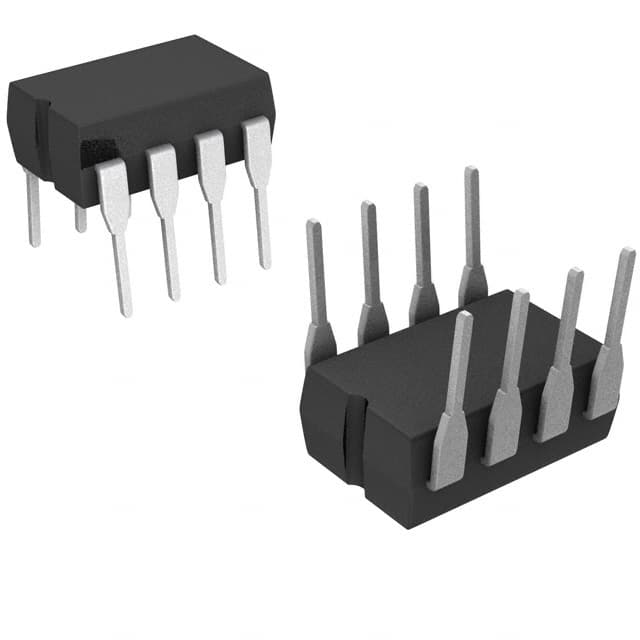
- Part No.:
- MAX667MJA/883B
- Manufacturer:
- Analog Devices Inc./Maxim Integrated
- Package:
- 8-CDIP (0.300", 7.62mm)
- Datasheet:
-
 MAX667MJA/883B.pdf
- Description:
- IC REG LIN POS ADJ 250MA 8CERDIP
- Quantity:
- Payment:

- Shipping:

Inventory:2,371
Please send an inquiry. Send us your inquiry, and we will respond immediately.
Product details
Overview
MAX667MJA/883B from Maxim Integrated is a military-grade, low-dropout linear voltage regulator delivering up to 250mA output current with typical dropout of 150mV at 200mA load. It features Dual Mode™ operation (fixed +5V or adjustable 1.3V–16V output), integrated low-battery detector (LBO/LBI), shutdown control (SHDN), and dropout detector (DD). It is used in high-reliability battery-powered instrumentation operating from -55°C to +125°C.
For engineers reviewing the MAX667MJA/883B datasheet, MAX667MJA/883B pinout, MAX667MJA/883B application, or MAX667MJA/883B equivalent, key selection criteria include guaranteed 250mA output under extended temperature, MIL-STD-883B qualified CERDIP-8 packaging, dual-mode programmability, sub-1µA shutdown quiescent current, and integrated power-fail warning functions.
Technical Context
The MAX667MJA/883B employs a PNP pass transistor architecture with micropower bandgap reference (1.225V ±25mV) and dual-comparator supervision circuitry. Its error amplifier compares either internal 5V divider or external SET-resistor feedback to regulate output.
It integrates three independent monitoring functions: LBI/LBO for low-battery detection (threshold referenced to 1.225V), SHDN for <1µA standby mode activation, and DD - an open-collector PNP output that sources increasing current as VIN–VOUT approaches ~300mV, providing early dropout warning.
Key Specifications
| Parameter | Value and Actual Design Meaning |
|---|---|
| Output Current | 250mA maximum - supports moderate-power analog/digital loads without external pass devices |
| Dropout Voltage | 150mV typical at 200mA - enables regulation down to VIN = VOUT + 0.15V, extending usable battery life |
| Quiescent Current | 20µA typical in normal mode; <1µA in SHDN mode - critical for multi-year battery operation |
| Input Voltage Range | +3.5V to +16.5V - accommodates single Li-ion, multi-cell alkaline, or wide-range industrial supplies |
| Operating Temperature | -55°C to +125°C - fully specified and tested per MIL-STD-883B, suitable for aerospace and defense platforms |
| SET Reference Voltage | 1.225V ±25mV - enables precise resistor-based output programming from 1.3V to 16V |
| LBI Threshold Voltage | 1.225V ±30mV - allows configurable low-battery warning via external resistive divider |
Pinout & Package
MAX667MJA/883B is supplied in an 8-pin CERDIP (Ceramic Dual In-line Package) with hermetic sealing and MIL-STD-883B qualification. The package is leaded, through-hole mountable, and rated for harsh-environment reliability.
| Pin/Terminal | Circuit Role | Design Meaning |
|---|---|---|
| 1 - DD | Dropout Detector Output | Open-collector PNP output sourcing current when VIN–VOUT falls below ~300mV; used for early regulation-loss warning |
| 2 - OUT | Regulated Output | Main power output; requires ≥10µF capacitor for stability; drops to 0V when SHDN is active |
| 3 - LBI | Low-Battery Input | CMOS input to internal 1.225V comparator; threshold set by external resistor divider |
| 4 - GND | Ground Reference | Analog and power ground return; must be low-impedance for stable regulation and accurate sensing |
| 5 - SHDN | Shutdown Control | CMOS input; pulled >1.5V to disable OUT/LBO/DD and reduce IQ to <1µA; max voltage = VIN + 0.3V |
| 6 - SET | Output Voltage Select | CMOS input; grounded for fixed +5V; >50mV above GND enables adjustable mode using external R-divider |
| 7 - LBO | Low-Battery Output | Open-drain N-channel output sinking current when LBI < 1.225V; requires external pull-up to ≤VOUT |
| 8 - IN | Unregulated Input | Positive supply input; absolute max +18V; must exceed VOUT by ≥dropout voltage for regulation |
Key Features
| Feature | Design Value |
|---|---|
| Dual Mode™ Operation | Single IC supports both minimal-component +5V fixed output (SET = GND) and precision-adjustable 1.3V–16V output (external R-divider on SET) |
| Integrated Power Supervision | Three independent functions - low-battery detection (LBI/LBO), dropout warning (DD), and shutdown control (SHDN) - reduce BOM count and board space |
| MIL-STD-883B Qualified | Tested per Method 5005 (Steady-State Life), 5007 (Thermal Shock), and 5011 (Burn-In); certified for high-reliability military/aerospace use |
| Ultra-Low Quiescent Current | 20µA typical in active mode; <1µA in SHDN - enables decade-scale battery life in always-on remote sensors |
| Robust Output Stability | Guaranteed stable with standard 10µF aluminum electrolytic capacitor; no ESR tuning required for most applications |
Applications
| Aerospace Telemetry Sensors | Defense Radios |
|---|---|
Use Scenario: Long-duration satellite payload sensors operating on primary lithium batteries in thermal vacuum environments. IC Role / Device Role / Timing Role: Primary 5V power regulator with end-of-life battery monitoring and graceful shutdown signaling. Use Value: -55°C to +125°C operation ensures functionality across orbital thermal cycles; DD and LBO outputs feed telemetry bus for predictive battery management. |
Use Scenario: Manpack tactical radios requiring reliable 5V rail under shock, vibration, and extreme ambient temperatures. IC Role / Device Role / Timing Role: Main system regulator with SHDN-controlled sleep mode and low-battery alert to conserve battery during standby. Use Value: MIL-qualified CERDIP-8 package withstands mechanical stress; <1µA shutdown current extends operational readiness between missions. |
| Downhole Oilfield Instrumentation | Strategic Missile Guidance Systems |
Use Scenario: High-temperature pressure/temperature sensors deployed in oil/gas wellbores exceeding 125°C ambient. IC Role / Device Role / Timing Role: Local 5V regulator powering ADCs and RF transceivers; LBI monitors battery health under thermal stress. Use Value: Guaranteed performance to +125°C eliminates derating concerns; 1.225V LBI reference remains stable across full temperature range. |
Use Scenario: Inertial measurement units (IMUs) requiring fail-safe power sequencing and regulation loss detection during launch and flight. IC Role / Device Role / Timing Role: Critical 5V supply with DD output feeding fault-detection logic to initiate safe mode before regulation collapse. Use Value: DD's abrupt current rise at ~300mV VIN–VOUT provides deterministic, temperature-stable dropout warning margin for real-time safety decisions. |
Equivalent & Alternatives
The following parts are listed as comparable options for similar low-dropout voltage regulator applications.
| Alternative Part | Technical Difference | Application Difference | Selection Advice |
|---|---|---|---|
| LM3940IT-5.0/NOPB | Fixed 5V only; 500mA output; higher 500mV dropout at 250mA; commercial temp range (–40°C to +125°C), not MIL-qualified | Lacks SET adjustability, LBO, DD, and MIL-STD-883B testing; suited for cost-sensitive industrial designs | Select if higher output current is needed and military qualification is unnecessary |
| LT1129CS8-5#PBF | Fixed 5V; 700mA output; 390mV dropout at 500mA; SO-8 package; no integrated LBO/DD/SHDN supervision | No built-in battery monitoring or shutdown; requires external circuitry for those functions; wider input range (3.5V–30V) | Select for higher current and lower dropout in non-military, surface-mount applications where supervision is added externally |
Compared with MAX667MJA/883B, LM3940IT-5.0/NOPB offers higher current but lacks military qualification and supervision features, while LT1129CS8-5#PBF provides lower dropout and higher current in SO-8 but requires external components for LBO/DD/SHDN functionality - neither matches the integrated, ruggedized, dual-mode capability of the MAX667MJA/883B.
Availability
MAX667MJA/883B is available at Aetrix Electronics and suitable for aerospace telemetry sensors, defense radios, downhole instrumentation, and strategic missile guidance systems requiring stable component supply across extended temperature and long lifecycle programs.
Supply support for MAX667MJA/883B includes scheduled delivery planning, volume procurement assistance, BOM continuity management, traceable sourcing, and lifecycle availability coordination for OEM customers, industrial embedded developers, connected-device designers, and electronics production programs.
Manufacturer
Maxim Integrated (now part of Analog Devices) is a U.S.-based semiconductor company specializing in high-performance analog, mixed-signal, and power management ICs for demanding applications.
The MAX667 belongs to Maxim's precision micropower linear regulator product line, designed specifically for battery-critical, high-reliability systems where extended temperature operation, ultra-low quiescent current, and integrated power supervision are mandatory.
FAQ
What is the maximum input voltage rating for the MAX667MJA/883B?
The MAX667MJA/883B has an absolute maximum input voltage rating of +18V. Operation beyond this voltage risks permanent device damage. For reliable continuous operation, the input should remain within the recommended range of +3.5V to +16.5V, as specified in the electrical characteristics table. This limit applies across the full -55°C to +125°C operating temperature range.
How does the SET pin determine output voltage in adjustable mode for the MAX667MJA/883B?
In adjustable mode, the MAX667MJA/883B uses the SET pin as the feedback node. When SET is held >50mV above GND, the internal error amplifier connects directly to SET instead of the internal 5V divider. With VSET = 1.225V ±25mV, the output voltage is calculated as VOUT = 1.225V × (R1 + R2)/R1, where R1 connects SET to GND and R2 connects OUT to SET. Typical R1 = 1MΩ ensures accuracy despite <10nA input bias current.
What is the function of the DD pin on the MAX667MJA/883B, and how is it used?
The DD (Dropout Detector) pin on the MAX667MJA/883B is an open-collector PNP output that begins sourcing current when VIN–VOUT falls below approximately 300mV. It provides early warning of impending regulation loss. A 100kΩ pull-down resistor converts DD current into a measurable voltage, which can be monitored by an ADC or comparator. This signal enables predictive shutdown or system state transition before VOUT collapses.
Is the MAX667MJA/883B pin-compatible with earlier versions like the MAX666?
Yes, the MAX667MJA/883B is explicitly described as a pin-compatible upgrade to the MAX666 in applications where input voltages exceed +3.5V. Both share identical 8-pin CERDIP packaging and pin assignments. However, the MAX667MJA/883B delivers higher output current (250mA vs. 150mA), lower dropout (150mV vs. ~350mV), and improved high-temperature performance - making it a direct functional replacement where those enhancements are beneficial.
What output capacitor is required for stable operation of the MAX667MJA/883B?
The MAX667MJA/883B requires a minimum 10µF output capacitor for stability, as confirmed in the Typical Operating Circuit and Applications Information sections. Aluminum electrolytic capacitors are recommended due to their sufficient ESR across temperature; tantalum or OS-CON types may be used with series resistance to meet minimum ESR requirements shown in Figure 4. No external compensation network is needed when using standard 10µF electrolytics.
MAX667MJA/883B Specifications
- Product attributes
- Attribute value
- Manufacturer:
- Analog Devices Inc./Maxim Integrated
- Series:
- -
- Package/Case:
- 8-CDIP (0.300", 7.62mm)
- Packaging:
- Tube
- Product Status:
- Active
- Output Configuration:
- Positive
- Output Type:
- Adjustable (Fixed)
- Number of Regulators:
- 1
- Voltage - Input (Max):
- 16.5V
- Voltage - Output (Min/Fixed):
- 1.3V (5V)
- Voltage - Output (Max):
- 16V
- Voltage Dropout (Max):
- 0.35V @ 200mA
- Current - Output:
- 250mA
- Current - Quiescent (Iq):
- 35 µA
- Current - Supply (Max):
- 20 mA
- PSRR:
- -
- Control Features:
- Dropout Detector, Enable, Low Battery Detection
- Protection Features:
- -
- Operating Temperature:
- -55°C ~ 125°C
- Grade:
- -
- Qualification:
- -
- Mounting Type:
- Through Hole
- Supplier Device Package:
- 8-CERDIP
MAX667MJA/883B FAQ
1.How can I place an order for MAX667MJA/883B through Aetrix?
Please submit a Request for Quotation (RFQ) for MAX667MJA/883B on Aetrix. Our sales agent will provide a competitive quotation and guide you through the order confirmation once you accept the terms.
2.Are the price and stock information for MAX667MJA/883B reliable?
The price and inventory of MAX667MJA/883B are updated periodically and may fluctuate due to market conditions. Stock and pricing data are typically refreshed every 24 hours. Quotation validity for MAX667MJA/883B is usually 5 days.
3.What payment methods are accepted for MAX667MJA/883B?
We accept Wire Transfer, PayPal, Credit Card, Western Union, MoneyGram, and Escrow for MAX667MJA/883B transactions.
Note: Certain payment methods may incur a processing fee.
4.How is shipping managed for MAX667MJA/883B?
MAX667MJA/883B orders can be shipped via leading logistics carriers, including DHL, UPS, FedEx, TNT, or Registered Mail.
Once your MAX667MJA/883B order is processed, you will receive an email with the shipment details and tracking number.
Note: Tracking information may take up to 24 hours to appear. Express delivery typically takes 3–5 business days.
5.How can I obtain technical support or documentation for MAX667MJA/883B?
For technical support, including MAX667MJA/883B datasheets, pinout diagrams, or application guidance, please contact our engineering support team. They can provide detailed documentation and assistance for your MAX667MJA/883B requirements.
6.How does Aetrix verify that MAX667MJA/883B is sourced from the original manufacturer or authorized distributors?
All MAX667MJA/883B products on Aetrix are procured from qualified distributors and authorized channels. Our dedicated quality assurance team conducts strict verification, including traceability checks and, if necessary, third-party testing. This ensures that MAX667MJA/883B meets industry standards.
7.What is the process for return or replacement of MAX667MJA/883B?
All MAX667MJA/883B units undergo pre-shipment inspection (PSI). If there is an issue with MAX667MJA/883B, returns or replacements are accepted under the following conditions:
1.Quantity discrepancies, incorrect items, or visible external defects (such as breakage or corrosion), acknowledged by Aetrix.
2.The issue is reported within 90 days of delivery.
3.The MAX667MJA/883B part is unused and in its original packaging.
Return procedure for MAX667MJA/883B:
1.Submit a request within 90 days.
2.Obtain a Return Material Authorization (RMA) from Aetrix.
MAX667MJA/883B Tags

-
MIC5504-1.8YM5-TR
Microchip Technology
-
MIC5504-3.3YM5-TR
Microchip Technology

-
MIC5365-3.0YC5-TR
Microchip Technology
-
MIC5365-1.8YC5-TR
Microchip Technology
-
MIC5365-2.5YC5-TR
Microchip Technology
-
MIC5365-3.3YC5-TR
Microchip Technology

-
MIC5365-3.3YD5-TR
Microchip Technology

-
MIC5317-3.3YM5-TR
Microchip Technology

-
TLV1117LV33DCYR
Texas Instruments

-
MIC5317-3.3YMT-TZ
Microchip Technology

-
MIC5528-3.3YMT-TR
Microchip Technology

-
TLV75801PDRVR
Texas Instruments
Tech Hub

An SR latch stores one bit through cross-coupled feedback. This engineering reference covers NOR and NAND implementations, truth tables, forbidden-state recovery, gated operation, switch debouncing, fa…

Latch circuits retain one bit through feedback. This technical reference covers SR and D latches, truth tables, transparency, timing limits, latch-versus-flip-flop behavior, applications and common log…

An engineering guide to LED driver operation, constant-current and constant-voltage outputs, linear and switching topologies, dimming, IC selection, calculations, replacement compatibility, and fault c…

Operational amplifier guide covering op amp basics, feedback, ideal vs real op amps, common configurations, buffer circuits, offset, bias current, gain-bandwidth, slew rate, rail-to-rail limits and sel…

Jumper cables guide covering safe connection order, red and black clamp placement, final ground connection, cable gauge, length, clamp quality, copper vs CCA cables, jump starter comparison and battery…

LDO regulator guide covering low dropout voltage, power dissipation, thermal design, PSRR, output noise, capacitor stability, adjustable LDO circuits, LDO vs buck converter and datasheet selection chec…

Conditional Access Module guide covering CAM meaning, CI/CI+ interface, smart card authorization, DVB security workflow, TV and set-top box compatibility, internal electronics, ESD protection, connecto…

Guide to electronic component obsolescence covering EOL risk, PCN/PDN notices, last-time buy planning, replacement options, form-fit-function validation, counterfeit risk and BOM lifecycle management.

18650 battery guide covering lithium-ion cell basics, 3.6V/3.7V voltage, 4.2V charging, mAh and Wh capacity, protected cells, chargers, BMS, series-parallel packs, holders, welding and sourcing checks.…

Hall effect sensor guide covering working principle, linear and digital sensors, Arduino circuits, current sensing, speed detection, automotive applications, A3144 examples, signal filtering and datash…


