
 My Inquiry
 My Account


Analog Devices Inc./Maxim Integrated MAX6725AKASDD3+T
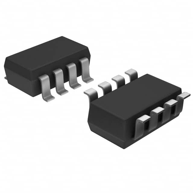
- Part No.:
- MAX6725AKASDD3+T
- Manufacturer:
- Analog Devices Inc./Maxim Integrated
- Category:
- Supervisors
- Package:
- SOT-23-8
- Datasheet:
-
 MAX6725AKASDD3+T.pdf
- Description:
- IC SUPERVISOR 3 CHANNEL SOT23-8
- Quantity:
- Payment:

- Shipping:

Inventory:3,197
Please send an inquiry. Send us your inquiry, and we will respond immediately.
Product details
Overview
The MAX6725AKASDD3+T from Maxim Integrated is a dual-supply microprocessor supervisory IC monitoring VCC1 (primary) and VCC2 (secondary) with factory-trimmed reset thresholds, 140ms minimum reset timeout, open-drain active-low RST output, manual-reset input (MR), and watchdog timer disable capability. It operates from -40°C to +125°C in an 8-pin SOT23 package and is used in telecom power management systems to ensure reliable cold-start and brownout recovery.
For engineers reviewing the MAX6725AKASDD3+T datasheet, MAX6725AKASDD3+T pinout, MAX6725AKASDD3+T application, or MAX6725AKASDD3+T equivalent, key selection criteria include dual-voltage monitoring down to 0.8V supply validity, guaranteed reset assertion during VCC1/VCC2 undervoltage events, 140ms timeout period (D3 suffix), and compatibility with 1.8V/3.3V multivoltage rail architectures.
Technical Context
This device implements independent voltage comparators for VCC1 and VCC2 with factory-trimmed thresholds (VTH1 = 4.625V typ, VTH2 = 3.075V typ), internal 140ms reset timeout timer, and logic-controlled reset assertion via MR or watchdog timeout. The reset output remains asserted until both supplies exceed their thresholds and the full timeout elapses.
It features a high-impedance MR input with 50kΩ internal pullup to VCC1, watchdog disable via floating WDI pin, and guaranteed valid reset state when either VCC1 or VCC2 ≥ 0.8V - enabling operation during deep brownout conditions without external support circuitry.
Key Specifications
| Parameter | Value and Actual Design Meaning |
|---|---|
| VCC1 Reset Threshold | 4.625V typical; ensures reset assertion before 5V system rail drops below critical logic margin. |
| VCC2 Reset Threshold | 3.075V typical; monitors 3.3V I/O supply with ±1.5% accuracy over temperature. |
| Reset Timeout Period | 140ms minimum (D3 suffix); provides sufficient hold time for FPGA/ASIC configuration and memory initialization. |
| Supply Current | 14µA typical at 3.6V; enables battery-backed operation in portable equipment with multi-year shelf life. |
| Operating Temperature | -40°C to +125°C; qualified for under-hood automotive and industrial control environments. |
| Reset Output Type | Open-drain active-low RST; allows wired-OR reset bus sharing across multiple supervisors or logic devices. |
| MR Input Logic | Active-low with 50kΩ internal pullup to VCC1; eliminates need for external resistor in manual-reset pushbutton circuits. |
Pinout & Package
Package: 8-pin SOT23 (K8SN+1 outline, 21-0078), surface-mount, RoHS-compliant, thermal resistance θJA = 180°C/W on multilayer board.
| Pin/Terminal | Circuit Role | Design Meaning |
|---|---|---|
| 1 | RST/RST1 | Active-low open-drain reset output referenced to VCC1; asserts when VCC1/VCC2 drop below threshold or MR is pulled low. |
| 2 | GND | Ground reference for all internal comparators, timers, and output drivers. |
| 3 | MR | Active-low manual-reset input with internal 50kΩ pullup to VCC1; initiates reset on falling edge and holds for full timeout after release. |
| 4 | VCC2 | Secondary supply input powering VCC2 comparator and RST2 output logic; also serves as reference for VCC2 threshold detection. |
| 5 | VCC1 | Primary supply input powering core logic, VCC1 comparator, and RST output driver; defines operating voltage range (0.8V–5.5V). |
| 6 | RSTIN | Adjustable reset comparator input with 626mV internal reference; enables third-voltage monitoring (e.g., 1.2V core) via external resistor divider. |
| 7 | PFI | Power-fail input with 626.5mV threshold; used to monitor preregulated supplies or battery voltage for orderly shutdown signaling. |
| 8 | PFO | Active-low open-drain power-fail output; asserts independently of reset timeout, enabling immediate interrupt generation without system reset. |
Key Features
| Feature | Design Value |
|---|---|
| Dual independent voltage monitoring | Simultaneous supervision of 5V primary and 3.3V secondary rails with separate thresholds and hysteresis. |
| 140ms reset timeout (D3) | Guaranteed minimum delay ensures complete processor boot sequence completion before release. |
| 0.8V supply validity guarantee | Reset logic remains functional even when VCC1 or VCC2 drops to 0.8V - critical for brownout resilience. |
| Watchdog disable by floating WDI | No external pullup required; internal 200nA current source detects unconnected state, simplifying design-in. |
| MR with integrated 50kΩ pullup | Reduces BOM count and PCB area by eliminating external resistor in pushbutton reset circuits. |
Applications
| Telecom Power Management | Industrial PLC Controller |
|---|---|
Use Scenario: Monitoring redundant 48V DC-DC converter outputs feeding 5V/3.3V system rails in carrier-grade base station power modules. IC Role / Device Role / Timing Role: Dual-rail supervisor asserting reset if either converter fails or experiences brownout, with 140ms hold time ensuring FPGA reconfiguration completes. Use Value: Prevents corrupted firmware load during unstable power-up, reducing field failure rate in mission-critical infrastructure. |
Use Scenario: Supervising 24V system supply and 5V I/O rail in programmable logic controller backplane with extended temperature operation. IC Role / Device Role / Timing Role: Provides fail-safe reset coordination between CPU and peripheral interface ICs during voltage sags caused by motor switching transients. Use Value: Eliminates need for discrete RC reset networks while maintaining AEC-Q100-equivalent reliability at +125°C ambient. |
| Server BMC Power Sequencing | Automotive ADAS Camera Module |
Use Scenario: Coordinating power-on reset timing between baseboard management controller (BMC) and host CPU in 1U rack server motherboards. IC Role / Device Role / Timing Role: Monitors BMC 3.3V rail and CPU 1.8V core rail, asserting shared reset bus only after both stabilize for ≥140ms. Use Value: Ensures deterministic boot order and prevents race conditions between BMC firmware and host BIOS initialization. |
Use Scenario: Supervising 12V input and 3.3V image sensor supply in rear-view camera ECU exposed to automotive underhood temperatures. IC Role / Device Role / Timing Role: Guarantees valid reset signal down to VCC1 = 0.8V during cold-crank battery dip, preventing sensor lockup. Use Value: Meets ISO 16750-2 pulse 4 requirements for transient immunity without additional protection circuitry. |
Equivalent & Alternatives
The following parts are listed as comparable options for similar dual-supply supervisory applications.
| Alternative Part | Technical Difference | Application Difference | Selection Advice |
|---|---|---|---|
| MAX6726AKASDD3+T | Push-pull RST output instead of open-drain; identical thresholds, timeout, and pinout. | Requires no external pullup resistor; unsuitable for wired-OR reset buses. | Select when driving single-load reset lines directly into µP reset pins without bus sharing. |
| TPS3808G33DBVR | Single-supply (3.3V only), no VCC2 monitoring; 200ms timeout; different pinout and no MR input. | Lacks dual-rail capability and manual reset; limited to 3.3V-only systems. | Choose only for cost-sensitive 3.3V-only designs where secondary rail supervision is unnecessary. |
Compared with MAX6725AKASDD3+T, MAX6726AKASDD3+T offers simplified drive but reduced bus flexibility, while TPS3808G33DBVR sacrifices dual-voltage monitoring and manual reset for lower unit cost in single-rail applications.
Availability
MAX6725AKASDD3+T is available at Aetrix Electronics and suitable for telecom power modules, industrial PLC controllers, and automotive ADAS camera modules requiring stable component supply across extended temperature ranges and long production lifecycles.
Supply support for MAX6725AKASDD3+T includes scheduled delivery planning, volume procurement assistance, BOM continuity management, traceable sourcing, and lifecycle availability coordination for OEM customers, industrial embedded developers, connected-device designers, and electronics production programs.
Manufacturer
Maxim Integrated (now part of Analog Devices) designs precision analog and mixed-signal ICs for demanding industrial, automotive, and communications applications.
The MAX6715A–MAX6729A family delivers ultra-low-voltage supervisory functions targeting multirail systems where simultaneous monitoring of primary and secondary supplies is essential for system-level reliability.
FAQ
What is the exact reset timeout period of the MAX6725AKASDD3+T?
The MAX6725AKASDD3+T has a guaranteed minimum reset timeout period of 140ms, corresponding to the 'D3' suffix in its part number. This value is specified over the full -40°C to +125°C operating temperature range and ensures sufficient hold time for complex processor initialization sequences before releasing the reset signal. The actual timeout may vary slightly due to process and temperature, but never falls below 140ms.
Does the MAX6725AKASDD3+T support monitoring a third voltage rail?
Yes, the MAX6725AKASDD3+T supports third-rail monitoring via its RSTIN pin, which features a precise 626mV internal reference voltage. By connecting an external resistor divider from VCCx to GND with RSTIN at the midpoint, users can configure custom reset thresholds down to 0.62V - enabling supervision of 1.2V, 1.0V, or other auxiliary supplies alongside the primary VCC1 and secondary VCC2 rails.
How does the manual-reset input (MR) function on the MAX6725AKASDD3+T?
The MR input on the MAX6725AKASDD3+T is an active-low signal with an internal 50kΩ pullup resistor to VCC1. Pulling MR low forces an immediate reset assertion, which remains active for the full 140ms timeout period after MR returns high. This allows direct connection to a momentary switch (MR to GND) without external components, and the 1µs minimum pulse width requirement ensures noise immunity against contact bounce.
Can the MAX6725AKASDD3+T operate reliably during severe supply brownouts?
Yes, the MAX6725AKASDD3+T guarantees valid reset output logic states down to VCC1 or VCC2 = 0.8V - significantly below typical logic thresholds. This enables robust operation during deep brownouts common in automotive cold-crank or industrial motor-start scenarios. The device maintains accurate voltage comparison and timer functionality even as supply voltages sag, ensuring deterministic reset behavior without external support circuitry.
What is the purpose of the PFI and PFO pins on the MAX6725AKASDD3+T?
The PFI (power-fail input) and PFO (power-fail output) pins on the MAX6725AKASDD3+T provide independent early-warning monitoring of a third supply, such as a battery or preregulated input. When PFI falls below its 626.5mV threshold, PFO asserts immediately (no timeout delay), allowing the system µP to execute an orderly shutdown routine before main rails collapse - a critical capability for data integrity in storage and telemetry applications.
MAX6725AKASDD3+T Specifications
- Product attributes
- Attribute value
- Manufacturer:
- Analog Devices Inc./Maxim Integrated
- Series:
- -
- Package/Case:
- SOT-23-8
- Packaging:
- Cut Tape (CT)
- Product Status:
- Active
- Programmable:
- Not Verified
- Type:
- Multi-Voltage Supervisor
- Number of Voltages Monitored:
- 3
- Voltage - Threshold:
- 0.788V, 2.925V, Adj
- Output:
- Open Drain, Open Drain
- Reset:
- Active High/Active Low
- Reset Timeout:
- 140ms Minimum
- Operating Temperature:
- -40°C ~ 125°C (TA)
- Grade:
- -
- Qualification:
- -
- Mounting Type:
- Surface Mount
- Supplier Device Package:
- SOT-23-8
MAX6725AKASDD3+T FAQ
1.How can I place an order for MAX6725AKASDD3+T through Aetrix?
Please submit a Request for Quotation (RFQ) for MAX6725AKASDD3+T on Aetrix. Our sales agent will provide a competitive quotation and guide you through the order confirmation once you accept the terms.
2.Are the price and stock information for MAX6725AKASDD3+T reliable?
The price and inventory of MAX6725AKASDD3+T are updated periodically and may fluctuate due to market conditions. Stock and pricing data are typically refreshed every 24 hours. Quotation validity for MAX6725AKASDD3+T is usually 5 days.
3.What payment methods are accepted for MAX6725AKASDD3+T?
We accept Wire Transfer, PayPal, Credit Card, Western Union, MoneyGram, and Escrow for MAX6725AKASDD3+T transactions.
Note: Certain payment methods may incur a processing fee.
4.How is shipping managed for MAX6725AKASDD3+T?
MAX6725AKASDD3+T orders can be shipped via leading logistics carriers, including DHL, UPS, FedEx, TNT, or Registered Mail.
Once your MAX6725AKASDD3+T order is processed, you will receive an email with the shipment details and tracking number.
Note: Tracking information may take up to 24 hours to appear. Express delivery typically takes 3–5 business days.
5.How can I obtain technical support or documentation for MAX6725AKASDD3+T?
For technical support, including MAX6725AKASDD3+T datasheets, pinout diagrams, or application guidance, please contact our engineering support team. They can provide detailed documentation and assistance for your MAX6725AKASDD3+T requirements.
6.How does Aetrix verify that MAX6725AKASDD3+T is sourced from the original manufacturer or authorized distributors?
All MAX6725AKASDD3+T products on Aetrix are procured from qualified distributors and authorized channels. Our dedicated quality assurance team conducts strict verification, including traceability checks and, if necessary, third-party testing. This ensures that MAX6725AKASDD3+T meets industry standards.
7.What is the process for return or replacement of MAX6725AKASDD3+T?
All MAX6725AKASDD3+T units undergo pre-shipment inspection (PSI). If there is an issue with MAX6725AKASDD3+T, returns or replacements are accepted under the following conditions:
1.Quantity discrepancies, incorrect items, or visible external defects (such as breakage or corrosion), acknowledged by Aetrix.
2.The issue is reported within 90 days of delivery.
3.The MAX6725AKASDD3+T part is unused and in its original packaging.
Return procedure for MAX6725AKASDD3+T:
1.Submit a request within 90 days.
2.Obtain a Return Material Authorization (RMA) from Aetrix.
MAX6725AKASDD3+T Tags
-
MIC826SYMT-TR
Microchip Technology

-
APX803S-31SA-7
Diodes Incorporated
-
APX803L20-29SA-7
Diodes Incorporated

-
TPS3828-33DBVR
Texas Instruments

-
V6340RSP3B+
EM Microelectronic
-
EM6325CXSP5B-2.9+
EM Microelectronic
-
MCP120T-300I/TT
Microchip Technology
-
MCP130T-315I/TT
Microchip Technology
-
MCP120T-475I/TT
Microchip Technology
-
MCP111T-300E/TT
Microchip Technology
-
MCP120T-315I/TT
Microchip Technology
-
MCP809T-315I/TT
Microchip Technology
Tech Hub

A practical engineering guide to 3.3V and 5V logic compatibility, input thresholds, resistor dividers, translator ICs, MOSFET level shifting, I2C pull-ups, timing limits and power-sequencing risks.

The 74HC595 uses push-pull logic outputs, while the TPIC6B595 uses 50 V open-drain DMOS sinks for higher-power loads. This guide compares timing, current limits, 3.3 V interfacing, load wiring, thermal…

The 74HC595 converts serial data into eight stable parallel outputs. This guide covers pin functions, shift and storage timing, OE and MR behavior, drive-current limits, cascading, voltage compatibilit…

A technical comparison of level-sensitive latches and edge-triggered flip-flops, covering timing windows, setup and hold limits, master–slave operation, time borrowing, race-through, HDL inference and…

A D latch stores one bit while Enable controls when data can pass. This reference covers gate-level operation, truth tables, transparency, setup and hold timing, LE versus OE, common ICs and practical …

An SR latch stores one bit through cross-coupled feedback. This engineering reference covers NOR and NAND implementations, truth tables, forbidden-state recovery, gated operation, switch debouncing, fa…

Latch circuits retain one bit through feedback. This technical reference covers SR and D latches, truth tables, transparency, timing limits, latch-versus-flip-flop behavior, applications and common log…

An engineering guide to LED driver operation, constant-current and constant-voltage outputs, linear and switching topologies, dimming, IC selection, calculations, replacement compatibility, and fault c…

Operational amplifier guide covering op amp basics, feedback, ideal vs real op amps, common configurations, buffer circuits, offset, bias current, gain-bandwidth, slew rate, rail-to-rail limits and sel…

Jumper cables guide covering safe connection order, red and black clamp placement, final ground connection, cable gauge, length, clamp quality, copper vs CCA cables, jump starter comparison and battery…


