
 My Inquiry
 My Account


Analog Devices Inc./Maxim Integrated MAX6757UTLD3+T
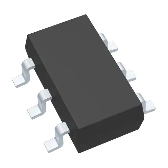
- Part No.:
- MAX6757UTLD3+T
- Manufacturer:
- Analog Devices Inc./Maxim Integrated
- Category:
- Supervisors
- Package:
- SOT-23-6
- Datasheet:
-
 MAX6757UTLD3+T.pdf
- Description:
- IC SUPERVISOR 1 CHANNEL SOT23-6
- Quantity:
- Payment:

- Shipping:

Inventory:2,738
Please send an inquiry. Send us your inquiry, and we will respond immediately.
Product details
Overview
MAX6757UTLD3+T from Analog Devices is a low-power, single-voltage window detector IC that monitors system supply voltage (VCC) for undervoltage and overvoltage conditions with independent push-pull UV and open-drain OV outputs, ±10% factory-trimmed thresholds at 3.3V nominal, 100ms minimum reset timeout, and manual reset input - used in telecom power supervision and server rail monitoring.
For engineers reviewing the MAX6757UTLD3+T datasheet, MAX6757UTLD3+T pinout, MAX6757UTLD3+T application, or MAX6757UTLD3+T equivalent, key selection criteria include its dual-output architecture, SOT23-6 package, -40°C to +125°C operation, 10μA supply current, and compatibility with 3.3V system rails requiring precise window detection with latch-free OV response.
Technical Context
The MAX6757UTLD3+T implements a fixed-threshold window detection architecture with separate internal comparators for UVTH and OVTH referenced to a precision bandgap, where SET pin configuration selects ±5%/±10%/±15% window width. Its UV output asserts when VCC falls below UVTH (2.970V–3.135V at 3.3V nominal), while OV asserts immediately when VCC exceeds OVTH (3.630V–3.795V) without timeout delay.
It features a 26kΩ internal MR pullup, 20μs propagation delay on MR assertion, and guaranteed output validity down to VCC = 1.0V - enabling reliable reset generation even during brownout recovery. The device operates across full industrial temperature range with <0.7% threshold hysteresis and immunity to transients ≥300ns.
Key Specifications
| Parameter | Value and Actual Design Meaning |
|---|---|
| Supply Voltage Range | 1.0V to 6.0V - supports operation and valid outputs even during deep brownout (VCC ≥ 1.0V). |
| UV Threshold (3.3V nominal) | 2.970V to 3.135V (falling VCC) - ±10% window centered at 3.3V, factory-trimmed. |
| OV Threshold (3.3V nominal) | 3.630V to 3.795V (rising VCC) - ±10% window centered at 3.3V, factory-trimmed. |
| Supply Current | 13μA typical at 3.6V - enables ultra-low-power system supervision in battery-backed or energy-constrained designs. |
| Timeout Period | 100ms minimum (D3 suffix) - ensures stable reset hold time after UV recovery, preventing premature processor release. |
| Operating Temperature | -40°C to +125°C - qualified for automotive under-hood, industrial control, and telecom base station environments. |
| Output Types | UV: active-low push-pull; OV: active-low open-drain - allows flexible interface to µP NMI/RESET pins and external pull-up networks. |
Pinout & Package
MAX6757UTLD3+T is housed in a 6-pin SOT23 package (package code U6+1, outline 21-0058), with thermal resistance θJA = 115°C/W on multilayer board - suitable for high-density PCB layouts with minimal thermal overhead.
| Pin/Terminal | Circuit Role | Design Meaning |
|---|---|---|
| 1 - GND | Ground reference | Primary return path for internal bias and output drivers; must be low-impedance connection to system ground plane. |
| 2 - UV | Undervoltage output | Active-low push-pull output asserting when VCC < UVTH; drives µP NMI or RESET directly without external pull-up. |
| 3 - MR | Manual reset input | Active-low input with 26kΩ internal pullup to VCC; initiates immediate UV assertion and holds for tMR_P (100–320ms). |
| 4 - SET | Window select input | Configures threshold window: tied to VCC for ±10%, GND for ±5%, or VCC/2 for ±15% - sets comparator hysteresis width. |
| 5 - OV | Overvoltage output | Active-low open-drain output asserting when VCC > OVTH; requires external pull-up for logic-level interface. |
| 6 - VCC | Power and monitored supply | Single-supply input powering the IC and serving as the monitored voltage rail; bypass with 0.1µF capacitor to GND. |
Key Features
| Feature | Design Value |
|---|---|
| Independent UV/OV outputs | Enables simultaneous fault signaling - e.g., UV triggers processor reset while OV activates crowbar circuit independently. |
| Factory-trimmed ±10% window at 3.3V | Eliminates external resistor networks; achieves ±1.5% total accuracy over temperature without calibration. |
| 100ms minimum timeout (D3) | Guarantees reset pulse width sufficient for full microprocessor initialization, even under slow-rising VCC conditions. |
| Low 10μA supply current | Reduces quiescent power in always-on supervision circuits - critical for battery-backed real-time clocks and watchdog systems. |
| Manual reset with 26kΩ pullup | Supports pushbutton-initiated system reset without external components; 4μs minimum pulse width ensures robust triggering. |
Applications
| Telecom Power Supervision | Server Rail Monitoring |
|---|---|
Use Scenario: Monitoring +3.3V bias rail in optical line terminal (OLT) power module to prevent FPGA configuration corruption during voltage sag. IC Role / Device Role / Timing Role: Window detector asserting UV output within 20μs of VCC falling below 2.97V, holding reset for ≥100ms until rail stabilizes. Use Value: Prevents partial configuration lockup by ensuring FPGA remains held in reset until supply meets timing margin requirements. | Use Scenario: Supervising 3.3V I/O rail in dual-CPU server motherboard where transient overvoltage could damage PCIe PHYs. IC Role / Device Role / Timing Role: OV output asserts immediately (<20μs) when VCC exceeds 3.795V, triggering fast-acting TVS clamp control. Use Value: Enables sub-100ns system-level overvoltage response by decoupling OV detection from reset timeout logic. |
| Industrial PLC Power Integrity | Automotive ADAS Domain Controller |
Use Scenario: Detecting brownout on 3.3V MCU core supply in programmable logic controller operating in -40°C ambient. IC Role / Device Role / Timing Role: UV output drives MCU NMI pin; guaranteed operation down to VCC = 1.0V ensures detection even during severe undervoltage events. Use Value: Maintains deterministic fault response across full industrial temperature range without derating or external compensation. | Use Scenario: Monitoring 3.3V sensor interface rail in radar ECU exposed to load-dump transients. IC Role / Device Role / Timing Role: Dual-output architecture separates UV (system reset) and OV (transient flag) functions - OV latches no, enabling transient event logging. Use Value: Supports ASIL-B diagnostic coverage by providing independent, timestampable UV and OV fault signals to safety MCU. |
Equivalent & Alternatives
The following parts are listed as comparable options for similar window detector applications.
| Alternative Part | Technical Difference | Application Difference | Selection Advice |
|---|---|---|---|
| MAX6757UTTD3+T | Same 3.3V nominal, but ±5% window (SET = GND) instead of ±10% (SET = VCC); identical pinout and timing. | Suitable where tighter threshold tolerance is required - e.g., 3.3V ±3% regulated rails with minimal margin. | Select MAX6757UTTD3+T only if system design mandates narrower window; otherwise MAX6757UTLD3+T provides better noise immunity. |
| TLV809E33DBZR | Single-output (reset only), no independent OV; ±2% accuracy, 200ms timeout; SOT23-3 package. | Lacks OV fault signaling - cannot support dual-fault diagnostics or crowbar activation in overvoltage scenarios. | Use TLV809E33DBZR only for cost-sensitive, single-fault applications where OV detection is handled externally. |
Compared with MAX6757UTTD3+T, the MAX6757UTLD3+T offers wider ±10% window for improved noise margin in noisy 3.3V systems, while TLV809E33DBZR reduces footprint and cost but sacrifices independent overvoltage monitoring capability essential for functional safety compliance.
Availability
MAX6757UTLD3+T is available at Aetrix Electronics and suitable for telecom power supervision, server rail monitoring, and industrial PLC power integrity applications requiring stable component supply across extended temperature ranges and long production lifecycles.
Supply support for MAX6757UTLD3+T includes scheduled delivery planning, volume procurement assistance, BOM continuity management, traceable sourcing, and lifecycle availability coordination for OEM customers, industrial embedded developers, connected-device designers, and electronics production programs.
Manufacturer
Analog Devices is a global leader in high-performance analog, mixed-signal, and digital signal processing semiconductors, serving industrial, automotive, communications, and healthcare markets.
The MAX6757UTLD3+T belongs to the MAX6754–MAX6764 family of low-power window detectors designed specifically for robust, single-rail voltage supervision in harsh environments with wide temperature and supply voltage ranges.
FAQ
What is the exact undervoltage threshold range for MAX6757UTLD3+T at 3.3V nominal supply?
The MAX6757UTLD3+T has a factory-trimmed undervoltage threshold range of 2.970V to 3.135V (falling VCC) at 3.3V nominal, corresponding to ±10% window with 2.5% hysteresis. This specification is guaranteed over -40°C to +125°C and applies specifically to the UTLD3 variant per Analog Devices datasheet revision 12.
Does MAX6757UTLD3+T support independent overvoltage and undervoltage outputs?
Yes, MAX6757UTLD3+T provides independent outputs: UV is an active-low push-pull output for undervoltage detection, and OV is an active-low open-drain output for overvoltage detection. This separation allows concurrent fault signaling without shared timing constraints - a defining feature of the MAX6757–MAX6764 series.
What package type and pin count does MAX6757UTLD3+T use?
MAX6757UTLD3+T uses a 6-pin SOT23 package (package code U6+1, outline number 21-0058). It is not available in TDFN or 5-pin variants - the 6-pin SOT23 is the only package offered for the MAX6757UTLD3+T part number, as confirmed in the official Analog Devices ordering information.
How does the SET pin configure the window width on MAX6757UTLD3+T?
On MAX6757UTLD3+T, the SET pin configures window width: connecting SET to VCC selects ±10% (L suffix), to GND selects ±5% (T suffix), and biasing to VCC/2 selects ±15%. The UTLD3+T variant is configured for ±10%, so SET must be tied to VCC for correct operation per datasheet Figure 2 and Pin Description table.
Is MAX6757UTLD3+T qualified for automotive applications?
MAX6757UTLD3+T is specified for -40°C to +125°C operation and meets extended temperature requirements for under-hood automotive use, but it is not AEC-Q100 qualified - only /V-suffixed parts in this family (e.g., MAX6757UTLD3/V) carry AEC-Q100 qualification. Designers requiring automotive qualification must select the /V variant.
MAX6757UTLD3+T Specifications
- Product attributes
- Attribute value
- Manufacturer:
- Analog Devices Inc./Maxim Integrated
- Series:
- -
- Package/Case:
- SOT-23-6
- Packaging:
- Tape & Reel (TR)
- Product Status:
- Obsolete
- Programmable:
- Not Verified
- Type:
- Simple Reset/Power-On Reset
- Number of Voltages Monitored:
- 1
- Voltage - Threshold:
- 5V
- Output:
- Push-Pull, Totem Pole
- Reset:
- Active Low
- Reset Timeout:
- 100ms Minimum
- Operating Temperature:
- -40°C ~ 125°C (TA)
- Grade:
- -
- Qualification:
- -
- Mounting Type:
- Surface Mount
- Supplier Device Package:
- SOT-6
MAX6757UTLD3+T FAQ
1.How can I place an order for MAX6757UTLD3+T through Aetrix?
Please submit a Request for Quotation (RFQ) for MAX6757UTLD3+T on Aetrix. Our sales agent will provide a competitive quotation and guide you through the order confirmation once you accept the terms.
2.Are the price and stock information for MAX6757UTLD3+T reliable?
The price and inventory of MAX6757UTLD3+T are updated periodically and may fluctuate due to market conditions. Stock and pricing data are typically refreshed every 24 hours. Quotation validity for MAX6757UTLD3+T is usually 5 days.
3.What payment methods are accepted for MAX6757UTLD3+T?
We accept Wire Transfer, PayPal, Credit Card, Western Union, MoneyGram, and Escrow for MAX6757UTLD3+T transactions.
Note: Certain payment methods may incur a processing fee.
4.How is shipping managed for MAX6757UTLD3+T?
MAX6757UTLD3+T orders can be shipped via leading logistics carriers, including DHL, UPS, FedEx, TNT, or Registered Mail.
Once your MAX6757UTLD3+T order is processed, you will receive an email with the shipment details and tracking number.
Note: Tracking information may take up to 24 hours to appear. Express delivery typically takes 3–5 business days.
5.How can I obtain technical support or documentation for MAX6757UTLD3+T?
For technical support, including MAX6757UTLD3+T datasheets, pinout diagrams, or application guidance, please contact our engineering support team. They can provide detailed documentation and assistance for your MAX6757UTLD3+T requirements.
6.How does Aetrix verify that MAX6757UTLD3+T is sourced from the original manufacturer or authorized distributors?
All MAX6757UTLD3+T products on Aetrix are procured from qualified distributors and authorized channels. Our dedicated quality assurance team conducts strict verification, including traceability checks and, if necessary, third-party testing. This ensures that MAX6757UTLD3+T meets industry standards.
7.What is the process for return or replacement of MAX6757UTLD3+T?
All MAX6757UTLD3+T units undergo pre-shipment inspection (PSI). If there is an issue with MAX6757UTLD3+T, returns or replacements are accepted under the following conditions:
1.Quantity discrepancies, incorrect items, or visible external defects (such as breakage or corrosion), acknowledged by Aetrix.
2.The issue is reported within 90 days of delivery.
3.The MAX6757UTLD3+T part is unused and in its original packaging.
Return procedure for MAX6757UTLD3+T:
1.Submit a request within 90 days.
2.Obtain a Return Material Authorization (RMA) from Aetrix.
MAX6757UTLD3+T Tags
-
MIC826SYMT-TR
Microchip Technology

-
APX803S-31SA-7
Diodes Incorporated
-
APX803L20-29SA-7
Diodes Incorporated

-
TPS3828-33DBVR
Texas Instruments

-
V6340RSP3B+
EM Microelectronic
-
EM6325CXSP5B-2.9+
EM Microelectronic
-
MCP120T-300I/TT
Microchip Technology
-
MCP130T-315I/TT
Microchip Technology
-
MCP120T-475I/TT
Microchip Technology
-
MCP111T-300E/TT
Microchip Technology
-
MCP120T-315I/TT
Microchip Technology
-
MCP809T-315I/TT
Microchip Technology
Tech Hub

A practical engineering guide to 3.3V and 5V logic compatibility, input thresholds, resistor dividers, translator ICs, MOSFET level shifting, I2C pull-ups, timing limits and power-sequencing risks.

The 74HC595 uses push-pull logic outputs, while the TPIC6B595 uses 50 V open-drain DMOS sinks for higher-power loads. This guide compares timing, current limits, 3.3 V interfacing, load wiring, thermal…

The 74HC595 converts serial data into eight stable parallel outputs. This guide covers pin functions, shift and storage timing, OE and MR behavior, drive-current limits, cascading, voltage compatibilit…

A technical comparison of level-sensitive latches and edge-triggered flip-flops, covering timing windows, setup and hold limits, master–slave operation, time borrowing, race-through, HDL inference and…

A D latch stores one bit while Enable controls when data can pass. This reference covers gate-level operation, truth tables, transparency, setup and hold timing, LE versus OE, common ICs and practical …

An SR latch stores one bit through cross-coupled feedback. This engineering reference covers NOR and NAND implementations, truth tables, forbidden-state recovery, gated operation, switch debouncing, fa…

Latch circuits retain one bit through feedback. This technical reference covers SR and D latches, truth tables, transparency, timing limits, latch-versus-flip-flop behavior, applications and common log…

An engineering guide to LED driver operation, constant-current and constant-voltage outputs, linear and switching topologies, dimming, IC selection, calculations, replacement compatibility, and fault c…

Operational amplifier guide covering op amp basics, feedback, ideal vs real op amps, common configurations, buffer circuits, offset, bias current, gain-bandwidth, slew rate, rail-to-rail limits and sel…

Jumper cables guide covering safe connection order, red and black clamp placement, final ground connection, cable gauge, length, clamp quality, copper vs CCA cables, jump starter comparison and battery…


