
 My Inquiry
 My Account


Analog Devices Inc./Maxim Integrated MAX8516EUB/V+
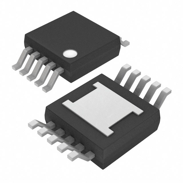
- Part No.:
- MAX8516EUB/V+
- Manufacturer:
- Analog Devices Inc./Maxim Integrated
- Package:
- 10-TFSOP, 10-MSOP (0.118", 3.00mm Width) Exposed Pad
- Datasheet:
-
 MAX8516EUB/V+.pdf
- Description:
- IC REG LINEAR POS ADJ 1A 10UMAX
- Quantity:
- Payment:

- Shipping:

Inventory:1,079
Please send an inquiry. Send us your inquiry, and we will respond immediately.
Product details
Overview
MAX8516EUB/V+ from Maxim Integrated is a low-dropout linear regulator with PMOS pass transistor architecture, delivering up to 1A output current from 1.425V–3.6V input while maintaining only 200mV dropout at full load. It features ±1.4% output voltage accuracy over 0°C to +85°C, 320μA typical ground current, and adjustable output from 0.5V to (VIN − 0.2V), widely deployed in post-regulation for high-efficiency server and optical module power rails.
For engineers reviewing the MAX8516EUB/V+ datasheet, MAX8516EUB/V+ pinout, MAX8516EUB/V+ application, or MAX8516EUB/V+ equivalent, key selection criteria include guaranteed 200mV dropout at 1A, ceramic-capacitor compatibility (1μF IN / 4.7μF OUT), soft-start inrush control, thermal-overload protection, and μMAX-10 package with exposed pad for thermal management.
Technical Context
The MAX8516EUB/V+ uses an internal p-channel MOSFET pass device with 100mΩ typical on-resistance, eliminating base-drive current and enabling stable operation down to 1.425V input without sacrificing transient response. Its feedback loop references a precise 500mV FB threshold with ±7mV accuracy over temperature and load.
It integrates undervoltage lockout (1.35V typ, 70mV hysteresis), logic-controlled shutdown (<25μA quiescent), short-circuit current limiting (1.6–2.4A), and thermal shutdown at +165°C (with +150°C hysteresis). Unlike NPN-based LDOs, supply current remains stable across load and dropout conditions due to zero gate-drive requirement.
Key Specifications
| Parameter | Value and Actual Design Meaning |
|---|---|
| Input Voltage Range | 1.425V to 3.6V - supports single-cell Li-ion, low-voltage logic rails, and intermediate bus architectures |
| Output Current | 1A continuous - sufficient for FPGA core rails, ASIC I/O banks, and high-speed SerDes supplies |
| Dropout Voltage | 200mV max at 1A - enables high-efficiency regulation even with minimal VIN–VOUT headroom |
| Output Accuracy | ±1.4% over line/load/temp (0°C to +85°C) - ensures reliable voltage margining for 1.2V/1.5V/1.8V digital loads |
| Ground Current | 320μA typ at 100mA load - ultra-low quiescent consumption critical for always-on subsystems |
| Shutdown Current | <25μA - enables deep-sleep power gating in portable and remote sensing applications |
| FB Threshold | 500mV ±3mV (typ) - enables accurate resistor-divider programming of any output from 0.5V to 3.4V |
| Capacitor Support | 1μF ceramic input / 4.7μF ceramic output - eliminates need for costly tantalum or electrolytic capacitors |
Pinout & Package
The MAX8516EUB/V+ is housed in a 10-pin μMAX® package (3mm × 5mm) with exposed thermal pad (EP) soldered to PCB ground for optimal power dissipation. Pin 10 is internally pulled down to GND via 10kΩ resistor and must be left floating.
| Pin/Terminal | Circuit Role | Design Meaning |
|---|---|---|
| 1 | EN | Logic-enable input - pull low for <25μA shutdown; connect to IN for always-on operation |
| 2, 3 | IN | Main input power rail - bypass with ≥1μF ceramic capacitor to GND for stability |
| 4, 5, 10 | N.C. | No connection - pins 4 & 5 are unused; pin 10 is internally pulled down, leave unconnected |
| 6 | GND | Power and signal ground - electrically and thermally coupled to EP for heat spreading |
| 7 | FB | Feedback reference node - connects to resistor divider to set output voltage (VFB = 500mV) |
| 8, 9 | OUT | Regulated output - bypass with ≥4.7μF ceramic capacitor to GND for 1A load stability |
| EP | GND (thermal) | Exposed pad - must be soldered to large PCB ground plane or multiple vias for thermal reliability |
Key Features
| Feature | Design Value |
|---|---|
| PMOS Pass Transistor | 100mΩ typical RDS(ON) - eliminates base-drive loss, enabling 340μA dropout current and stable low-VIN operation |
| Soft-Start Circuitry | Inherent ramp-up limits inrush current - prevents input rail sag and avoids false triggering of upstream protection |
| Thermal Shutdown | +165°C trip with +15°C hysteresis - protects against sustained overload or poor heatsinking without latch-up |
| Short-Circuit Protection | Current-limited to 1.6–2.4A - sustains indefinite short-circuit while limiting junction temperature rise |
| Ceramic Capacitor Optimized | Stable with 1μF CIN/4.7μF COUT - reduces BOM cost, footprint, and ESL vs. electrolytic alternatives |
| Undervoltage Lockout | 1.35V threshold with 70mV hysteresis - prevents erratic startup during brownout or battery discharge |
Applications
| Server Core Rails | Optical Module Bias |
|---|---|
Use Scenario: Regulating 1.2V/1.5V core supplies for Xeon Scalable CPUs and DDR5 memory controllers in 1U rack servers. IC Role / Device Role / Timing Role: Post-regulator providing clean, low-noise, tightly regulated voltage after primary DC/DC conversion. Use Value: 200mV dropout preserves efficiency under high ambient temperature; ±1.4% accuracy ensures timing margin compliance for high-speed interfaces. |
Use Scenario: Powering laser diode drivers and transimpedance amplifiers in 100G/400G QSFP-DD optical transceivers. IC Role / Device Role / Timing Role: Low-noise local regulator isolating analog bias rails from noisy digital switching noise. Use Value: High PSRR (>60dB @ 1kHz) and fast transient response (45mV deviation for 20mA→1A step) maintain signal integrity in high-bandwidth data links. |
| Base Station Fronthaul | Notebook SoC I/O |
Use Scenario: Supplying 1.8V/2.5V rails to RF front-end ICs and JESD204B serializer/deserializer in 5G massive MIMO active antennas. IC Role / Device Role / Timing Role: Point-of-load regulator delivering stable voltage despite wide input variation from PoE++ or hybrid AC/DC sources. Use Value: 1.425V minimum input supports operation during PoE voltage sag; thermal pad enables conduction cooling in sealed enclosures. |
Use Scenario: Generating 3.3V/1.8V I/O supplies for Intel Core i7/i9 and AMD Ryzen mobile processors in ultrabooks. IC Role / Device Role / Timing Role: Secondary LDO managing dynamic voltage scaling and low-power states for display interface and PCIe lanes. Use Value: <25μA shutdown current extends battery life in S0ix sleep modes; soft-start prevents system reset during resume transitions. |
Equivalent & Alternatives
The following parts are listed as comparable options for similar LDO regulator applications.
| Alternative Part | Technical Difference | Application Difference | Selection Advice |
|---|---|---|---|
| TPS7A4700RGWR | 20V max input, 1A, 300mV dropout, 4μVRMS noise - higher input range but larger dropout and no automotive qualification | Preferred for industrial analog rails requiring ultra-low noise; not suitable for sub-1.5V input or AEC-Q200 environments | Select TPS7A4700RGWR only when >3.6V input or sub-10μV noise is required; MAX8516EUB/V+ better fits low-VIN, automotive-grade space |
| MCP1826T-1202E/DB | 1.2V fixed output, 1A, 350mV dropout, SOT-223 package - no adjustability, higher dropout, no exposed thermal pad | Suitable for cost-sensitive consumer designs where fixed 1.2V and board space allow SOT-223; lacks thermal performance for sustained 1A | Choose MCP1826T-1202E/DB for non-adjustable, non-automotive, low-cost use; MAX8516EUB/V+ preferred for design flexibility, thermal robustness, and AEC-Q200 compliance |
Compared with TPS7A4700RGWR and MCP1826T-1202E/DB, the MAX8516EUB/V+ uniquely combines 1.425V minimum input, 200mV dropout at 1A, adjustable output, μMAX-10 thermal package, and automotive qualification - making it the only option meeting all four requirements simultaneously for compact, high-reliability embedded power rails.
Availability
MAX8516EUB/V+ is available at Aetrix Electronics and suitable for server power delivery, optical transceiver biasing, and 5G base station fronthaul requiring stable component supply, RoHS-compliant packaging, and automotive-grade reliability.
Supply support for MAX8516EUB/V+ includes scheduled delivery planning, volume procurement assistance, BOM continuity management, traceable sourcing, and lifecycle availability coordination for OEM customers, industrial embedded developers, connected-device designers, and electronics production programs.
Manufacturer
Maxim Integrated, now part of Analog Devices, designs precision analog, mixed-signal, and power management ICs for demanding industrial, communications, and automotive applications.
The MAX8516EUB/V+ belongs to Maxim's high-performance LDO family targeting low-input, low-dropout regulation in space-constrained, thermally challenging systems - specifically engineered for post-regulation in servers, optical modules, and wireless infrastructure.
FAQ
What is the minimum input voltage required for stable operation of the MAX8516EUB/V+?
The MAX8516EUB/V+ requires a minimum input voltage of 1.425V for guaranteed specification compliance across temperature and load. Below this, undervoltage lockout activates at 1.35V (typ) with 70mV hysteresis. Operation below 1.425V may occur but is not characterized - the MAX8516EUB/V+ is designed to deliver full 1A output only when VIN ≥ 1.425V and VOUT ≤ (VIN − 0.2V).
Does the MAX8516EUB/V+ support adjustable output voltage, and how is it configured?
Yes, the MAX8516EUB/V+ supports fully adjustable output from 0.5V to 3.4V using an external resistor divider connected to the FB pin. The feedback threshold is precisely 500mV (±3mV), so VOUT = 0.5V × (1 + R1/R2). For optimal accuracy and quiescent current, R2 should be ≤ 5kΩ. The MAX8516EUB/V+ does not offer fixed-output variants - adjustment is mandatory via external resistors.
What thermal management is required for the MAX8516EUB/V+ at 1A continuous load?
The MAX8516EUB/V+ requires soldering its exposed thermal pad (EP) to a solid PCB ground plane with multiple thermal vias to maintain safe junction temperature. At TA = +70°C, maximum continuous power dissipation is 824mW (derated above +70°C). With 1A load and 300mV dropout, power dissipation is 300mW - well within limit if EP is properly connected. Without EP grounding, thermal resistance rises sharply, risking thermal shutdown above ~600mA.
How does the enable (EN) pin function on the MAX8516EUB/V+?
The EN pin on the MAX8516EUB/V+ is an active-high logic input. Pulling EN low places the device in shutdown mode, reducing ground current to <25μA and disabling the output. For always-on operation, EN must be tied to IN. During shutdown, an internal 10kΩ resistor pulls the output toward GND - this is intentional and ensures safe discharge of downstream capacitance. EN has ±1μA bias current and 1.2V rising threshold.
Is the MAX8516EUB/V+ qualified for automotive applications, and what does the "/V+" suffix indicate?
Yes, the "/V+" suffix in MAX8516EUB/V+ explicitly denotes AEC-Q200 qualification and lead(Pb)-free/RoHS-compliant packaging. This version meets automotive reliability standards including extended temperature operation (−40°C to +85°C), robust ESD tolerance, and rigorous qualification testing. The base MAX8516EUB (without /V+) is commercial grade only - the /V+ variant is the sole automotive-qualified version in this family.
MAX8516EUB/V+ Specifications
- Product attributes
- Attribute value
- Manufacturer:
- Analog Devices Inc./Maxim Integrated
- Series:
- -
- Package/Case:
- 10-TFSOP, 10-MSOP (0.118", 3.00mm Width) Exposed Pad
- Packaging:
- Tube
- Product Status:
- Obsolete
- Output Configuration:
- Positive
- Output Type:
- Adjustable
- Number of Regulators:
- 1
- Voltage - Input (Max):
- 3.6V
- Voltage - Output (Min/Fixed):
- 0.5V
- Voltage - Output (Max):
- 3.4V
- Voltage Dropout (Max):
- 0.2V @ 1A
- Current - Output:
- 1A
- Current - Quiescent (Iq):
- 320 µA
- Current - Supply (Max):
- -
- PSRR:
- -
- Control Features:
- -
- Protection Features:
- Over Temperature, Short Circuit, Soft Start, Under Voltage Lockout (UVLO)
- Operating Temperature:
- -40°C ~ 85°C
- Grade:
- Automotive
- Qualification:
- AEC-Q100
- Mounting Type:
- Surface Mount
- Supplier Device Package:
- 10-uMAX-EP
MAX8516EUB/V+ FAQ
1.How can I place an order for MAX8516EUB/V+ through Aetrix?
Please submit a Request for Quotation (RFQ) for MAX8516EUB/V+ on Aetrix. Our sales agent will provide a competitive quotation and guide you through the order confirmation once you accept the terms.
2.Are the price and stock information for MAX8516EUB/V+ reliable?
The price and inventory of MAX8516EUB/V+ are updated periodically and may fluctuate due to market conditions. Stock and pricing data are typically refreshed every 24 hours. Quotation validity for MAX8516EUB/V+ is usually 5 days.
3.What payment methods are accepted for MAX8516EUB/V+?
We accept Wire Transfer, PayPal, Credit Card, Western Union, MoneyGram, and Escrow for MAX8516EUB/V+ transactions.
Note: Certain payment methods may incur a processing fee.
4.How is shipping managed for MAX8516EUB/V+?
MAX8516EUB/V+ orders can be shipped via leading logistics carriers, including DHL, UPS, FedEx, TNT, or Registered Mail.
Once your MAX8516EUB/V+ order is processed, you will receive an email with the shipment details and tracking number.
Note: Tracking information may take up to 24 hours to appear. Express delivery typically takes 3–5 business days.
5.How can I obtain technical support or documentation for MAX8516EUB/V+?
For technical support, including MAX8516EUB/V+ datasheets, pinout diagrams, or application guidance, please contact our engineering support team. They can provide detailed documentation and assistance for your MAX8516EUB/V+ requirements.
6.How does Aetrix verify that MAX8516EUB/V+ is sourced from the original manufacturer or authorized distributors?
All MAX8516EUB/V+ products on Aetrix are procured from qualified distributors and authorized channels. Our dedicated quality assurance team conducts strict verification, including traceability checks and, if necessary, third-party testing. This ensures that MAX8516EUB/V+ meets industry standards.
7.What is the process for return or replacement of MAX8516EUB/V+?
All MAX8516EUB/V+ units undergo pre-shipment inspection (PSI). If there is an issue with MAX8516EUB/V+, returns or replacements are accepted under the following conditions:
1.Quantity discrepancies, incorrect items, or visible external defects (such as breakage or corrosion), acknowledged by Aetrix.
2.The issue is reported within 90 days of delivery.
3.The MAX8516EUB/V+ part is unused and in its original packaging.
Return procedure for MAX8516EUB/V+:
1.Submit a request within 90 days.
2.Obtain a Return Material Authorization (RMA) from Aetrix.
MAX8516EUB/V+ Tags

-
MIC5504-1.8YM5-TR
Microchip Technology
-
MIC5504-3.3YM5-TR
Microchip Technology

-
MIC5365-3.0YC5-TR
Microchip Technology
-
MIC5365-1.8YC5-TR
Microchip Technology
-
MIC5365-2.5YC5-TR
Microchip Technology
-
MIC5365-3.3YC5-TR
Microchip Technology

-
MIC5365-3.3YD5-TR
Microchip Technology

-
MIC5317-3.3YM5-TR
Microchip Technology

-
TLV1117LV33DCYR
Texas Instruments

-
MIC5317-3.3YMT-TZ
Microchip Technology

-
MIC5528-3.3YMT-TR
Microchip Technology

-
TLV75801PDRVR
Texas Instruments
Tech Hub

An SR latch stores one bit through cross-coupled feedback. This engineering reference covers NOR and NAND implementations, truth tables, forbidden-state recovery, gated operation, switch debouncing, fa…

Latch circuits retain one bit through feedback. This technical reference covers SR and D latches, truth tables, transparency, timing limits, latch-versus-flip-flop behavior, applications and common log…

An engineering guide to LED driver operation, constant-current and constant-voltage outputs, linear and switching topologies, dimming, IC selection, calculations, replacement compatibility, and fault c…

Operational amplifier guide covering op amp basics, feedback, ideal vs real op amps, common configurations, buffer circuits, offset, bias current, gain-bandwidth, slew rate, rail-to-rail limits and sel…

Jumper cables guide covering safe connection order, red and black clamp placement, final ground connection, cable gauge, length, clamp quality, copper vs CCA cables, jump starter comparison and battery…

LDO regulator guide covering low dropout voltage, power dissipation, thermal design, PSRR, output noise, capacitor stability, adjustable LDO circuits, LDO vs buck converter and datasheet selection chec…

Conditional Access Module guide covering CAM meaning, CI/CI+ interface, smart card authorization, DVB security workflow, TV and set-top box compatibility, internal electronics, ESD protection, connecto…

Guide to electronic component obsolescence covering EOL risk, PCN/PDN notices, last-time buy planning, replacement options, form-fit-function validation, counterfeit risk and BOM lifecycle management.

18650 battery guide covering lithium-ion cell basics, 3.6V/3.7V voltage, 4.2V charging, mAh and Wh capacity, protected cells, chargers, BMS, series-parallel packs, holders, welding and sourcing checks.…

Hall effect sensor guide covering working principle, linear and digital sensors, Arduino circuits, current sensing, speed detection, automotive applications, A3144 examples, signal filtering and datash…


