
 My Inquiry
 My Account


Analog Devices Inc./Maxim Integrated MAX8883EUTGG-T
- Part No.:
- MAX8883EUTGG-T
- Manufacturer:
- Analog Devices Inc./Maxim Integrated
- Package:
- SOT-23-6
- Datasheet:
-
 MAX8883EUTGG-T.pdf
- Description:
- IC REG LINEAR LDO
- Quantity:
- Payment:

- Shipping:

Inventory:2,500
Please send an inquiry. Send us your inquiry, and we will respond immediately.
Product details
Overview
MAX8883EUTGG-T from Maxim Integrated is a dual low-noise, low-dropout linear regulator with independent shutdown control for each output, delivering 3.0V/3.0V at up to 160mA per channel from a +2.5V to +6.5V input. It features 72mV dropout at 80mA load, 165µA quiescent current (both LDOs active), and 60dB PSRR at 100Hz - optimized for battery-powered µP/DSP core/IO power in handheld instruments and digital cameras.
For engineers reviewing the MAX8883EUTGG-T datasheet, MAX8883EUTGG-T pinout, MAX8883EUTGG-T application, or MAX8883EUTGG-T equivalent, key selection criteria include dual independent shutdown logic, guaranteed 3.0V ±2% output accuracy over –40°C to +85°C, SOT23-6 package thermal performance, and low-noise operation without external BP capacitor dependency (unlike MAX8882).
Technical Context
The MAX8883EUTGG-T integrates two independent P-channel MOSFET pass transistors (RDS(ON) ≈ 1Ω), enabling load-proportional dropout voltage and eliminating base-drive current loss typical of PNP-based regulators. Each LDO has dedicated SHDNA/SHDNB inputs with 0.4V VIL and 1.6V VIH, supporting direct microcontroller GPIO control.
It implements independent current limiting (160mA min guaranteed per channel), thermal shutdown at +160°C with 10°C hysteresis, and short-circuit protection with indefinite fault tolerance. Unlike the MAX8882, it omits the BP pin and reference bypass path, trading noise optimization (320µVRMS) for simplified layout and dual-control flexibility.
Key Specifications
| Parameter | Value and Actual Design Meaning |
|---|---|
| Output Voltage (A/B) | 3.0V / 3.0V, fixed, ±2% accuracy over full temperature range - ensures stable core/IO rail matching for dual-domain processors. |
| Max Output Current | 160mA per channel continuous - supports moderate-power peripherals like image sensors or RF front-ends without derating. |
| Dropout Voltage | 72mV at 80mA load - enables >95% efficiency at light-to-moderate loads with 3.3V input, extending battery life in portable devices. |
| Quiescent Current | 165µA (both LDOs active), 10nA (both shutdown) - maintains ultra-low standby power for always-on subsystems. |
| PSRR | 60dB at 100Hz - suppresses low-frequency switching noise from upstream DC/DC converters feeding the LDO input. |
| Output Noise | 320µVRMS (10Hz–100kHz) - suitable for analog-sensitive circuits like ADC references or audio codecs where sub-mV ripple is critical. |
| Thermal Shutdown | Activates at +160°C with 10°C hysteresis - protects against sustained overload in compact SOT23-6 layouts with limited copper area. |
Pinout & Package
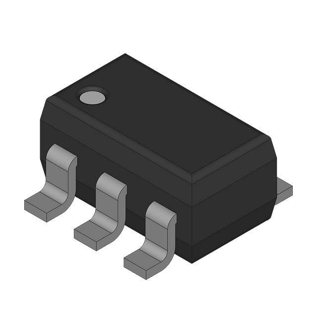
MAX8883EUTGG-T is housed in a thermally enhanced 6-pin SOT23-6 package (JEDEC MO-178AA). The GND pin serves as both electrical return and primary thermal path - requires soldering to ≥25 mm² copper pour for rated 160mA operation.
| Pin/Terminal | Circuit Role | Design Meaning |
|---|---|---|
| OUTB (Pin 1) | Regulator B output | Sources up to 160mA; requires 2.2µF ceramic output capacitor (X5R/X7R) for stability across –40°C to +85°C. |
| GND (Pin 2) | Power ground & thermal pad | Primary heat dissipation path; must connect to large PCB ground plane to maintain TJ ≤ +150°C at full load. |
| SHDNA (Pin 3) | Shutdown A control input | Logic-low (≤0.4V) disables OUTA only; high-impedance input draws <0.05nA - compatible with 1.8V/3.3V GPIOs. |
| SHDNB (Pin 4) | Shutdown B control input | Logic-low (≤0.4V) disables OUTB only; independent of SHDNA - enables asymmetric power sequencing. |
| IN (Pin 5) | Input supply | Accepts +2.5V to +6.5V; requires 2.2µF input capacitor to limit VIN ripple and support transient response. |
| OUTA (Pin 6) | Regulator A output | Sources up to 160mA; identical electrical specs to OUTB - allows symmetrical dual-rail generation from single input. |
Key Features
| Feature | Design Value |
|---|---|
| Dual independent shutdown | SHDNA/SHDNB pins enable selective power gating of each LDO - reduces system-level standby current without firmware coordination. |
| P-channel MOSFET pass devices | Eliminates base-drive current loss and saturation voltage penalty - delivers consistent 165µA quiescent current across all load conditions. |
| Guaranteed current limiting | 160mA minimum per channel - prevents damage during output shorts while maintaining predictable fault behavior for safety-critical designs. |
| Thermal shutdown with hysteresis | +160°C trip point with 10°C cooldown gap - avoids oscillation during marginal thermal conditions and enables self-recovery after transient overloads. |
| No BP pin required | Omits reference bypass terminal - simplifies PCB layout and eliminates risk of BP capacitor placement errors that degrade noise performance in MAX8882 variants. |
Applications
| Digital Camera Sensor Power | Hand-Held Instrument Dual-Rail Supply |
|---|---|
Use Scenario: Powers CMOS image sensor (3.0V analog core) and ISP processor I/O (3.0V digital interface) from a single Li-ion cell. IC Role / Device Role / Timing Role: Dual-output LDO providing isolated, low-noise rails with independent enable control for power sequencing during wake/sleep transitions. Use Value: 320µVRMS noise prevents fixed-pattern noise in captured images; 72mV dropout extends usable battery range by 120mV per cell. | Use Scenario: Supplies 3.0V to precision ADC front-end and 3.0V to microcontroller I/O bank in battery-operated multimeter. IC Role / Device Role / Timing Role: Dual LDO delivering matched, stable voltages with independent shutdown to minimize total system standby current. Use Value: 10nA dual-shutdown current enables >1-year shelf life; ±2% output accuracy ensures measurement repeatability across temperature. |
| µP Core/IO Split Rail | PDAs and Palmtop Computers |
Use Scenario: Generates separate 3.0V rails for ARM Cortex-M4 core (low-noise analog domain) and its 3.0V I/O bank in wearable health monitor. IC Role / Device Role / Timing Role: Dual LDO with independent enable pins allowing dynamic core voltage scaling while keeping I/O powered for peripheral communication. Use Value: Independent SHDNA/SHDNB control enables real-time power state management without additional level shifters or discrete FETs. | Use Scenario: Provides 3.0V main system rail and 3.0V backlight driver bias in legacy PDA with tight board space constraints. IC Role / Device Role / Timing Role: Compact dual LDO replacing two discrete regulators - reduces component count and improves layout efficiency in 6-pin SOT23 footprint. Use Value: SOT23-6 package occupies 30% less area than two 5-pin SOT23 LDOs; 165µA quiescent current extends runtime in always-on calendar/alert functions. |
Equivalent & Alternatives
The following parts are listed as comparable options for similar dual-LDO applications.
| Alternative Part | Technical Difference | Application Difference | Selection Advice |
|---|---|---|---|
| MAX8882EUTGG-T | Single SHDN pin; includes BP pin for 40µVRMS noise (vs. 320µVRMS); same 3.0V/3.0V outputs and SOT23-6 package. | Requires external 0.01µF BP capacitor for lowest noise; lacks independent shutdown - forces simultaneous enable/disable of both outputs. | Select when ultra-low noise is critical and dual-rail sequencing is unnecessary. |
| TSM1024IYPT | 3.3V/3.3V dual LDO; 250mA per channel; 200mV dropout at 150mA; no independent shutdown; SO-8 package. | Larger footprint and higher dropout reduce battery efficiency; higher current rating exceeds requirement but adds cost and size. | Select only if 3.3V rails and higher current headroom are needed - not drop-in due to voltage mismatch and package change. |
Compared with MAX8882EUTGG-T, the MAX8883EUTGG-T trades 280µVRMS higher noise for essential independent shutdown control and simpler layout. Against TSM1024IYPT, it offers superior dropout performance and smaller footprint but requires voltage-matched system design.
Availability
MAX8883EUTGG-T is available at Aetrix Electronics and suitable for digital camera sensor power, hand-held instrument dual-rail supply, and µP core/IO split-rail applications requiring stable component supply, long-term lifecycle assurance, and traceable sourcing.
Supply support for MAX8883EUTGG-T includes scheduled delivery planning, volume procurement assistance, BOM continuity management, traceable sourcing, and lifecycle availability coordination for OEM customers, industrial embedded developers, connected-device designers, and electronics production programs.
Manufacturer
Maxim Integrated (now part of Analog Devices) designs precision analog, mixed-signal, and power management ICs for demanding industrial, medical, and portable applications.
The MAX8882/MAX8883 product line targets battery-powered systems needing dual, low-noise, low-quiescent-current regulation in minimal footprint - specifically addressing µP/DSP core/IO separation and handheld instrumentation requirements.
FAQ
What output voltages does the MAX8883EUTGG-T provide?
The MAX8883EUTGG-T provides fixed 3.0V on both OUTA and OUTB outputs, with guaranteed ±2% accuracy over the full –40°C to +85°C operating temperature range. This dual 3.0V configuration is laser-trimmed at wafer test and does not require external feedback resistors. The top-mark "AAZU" on the SOT23-6 package confirms the 3.0V/3.0V variant.
Does the MAX8883EUTGG-T require an external bypass capacitor like the MAX8882?
No, the MAX8883EUTGG-T does not include a BP (bypass) pin and therefore does not require or support an external 0.01µF reference bypass capacitor. Its output noise is specified at 320µVRMS (10Hz–100kHz) without BP - higher than the MAX8882's 40µVRMS but sufficient for most digital and mixed-signal applications where independent shutdown is prioritized over ultra-low noise.
How does shutdown work on the MAX8883EUTGG-T?
The MAX8883EUTGG-T uses two independent logic-controlled inputs: SHDNA (Pin 3) shuts down only OUTA, and SHDNB (Pin 4) shuts down only OUTB. Driving either pin low (≤0.4V) disables its respective regulator while the other remains active. Driving both low reduces total supply current to 10nA. For normal operation, both pins must be tied to IN or a logic-high voltage.
What is the maximum continuous output current per channel for the MAX8883EUTGG-T?
The MAX8883EUTGG-T delivers up to 160mA continuous output current per channel (OUTA and OUTB), with guaranteed minimum current limiting at 160mA. This rating assumes proper thermal management - the SOT23-6 package requires connection of the GND pin to ≥25 mm² copper area to sustain 160mA at +85°C ambient without exceeding the +150°C junction limit.
Is the MAX8883EUTGG-T pin-compatible with the MAX8882 series?
No, the MAX8883EUTGG-T is not pin-compatible with MAX8882 variants. While both use SOT23-6 packages, the pin assignments differ: MAX8883 replaces the MAX8882's shared SHDN and BP pins with dedicated SHDNA and SHDNB pins (Pins 3 and 4). Swapping them without PCB revision will result in incorrect shutdown behavior and missing functionality - redesign is required for migration.
MAX8883EUTGG-T Specifications
- Product attributes
- Attribute value
- Manufacturer:
- Analog Devices Inc./Maxim Integrated
- Series:
- -
- Package/Case:
- SOT-23-6
- Packaging:
- Bulk
- Product Status:
- Active
- Output Configuration:
- Positive
- Output Type:
- Fixed
- Number of Regulators:
- 2
- Voltage - Input (Max):
- 6.5V
- Voltage - Output (Min/Fixed):
- 3.3V, 3.3V
- Voltage - Output (Max):
- -
- Voltage Dropout (Max):
- 0.144V @ 80mA
- Current - Output:
- 160mA, 160mA
- Current - Quiescent (Iq):
- 265 µA
- Current - Supply (Max):
- -
- PSRR:
- 10dB (100Hz)
- Control Features:
- Enable
- Protection Features:
- Over Current, Over Temperature, Short Circuit
- Operating Temperature:
- -40°C ~ 85°C (TA)
- Grade:
- -
- Qualification:
- -
- Mounting Type:
- Surface Mount
- Supplier Device Package:
- SOT-23-6
MAX8883EUTGG-T FAQ
1.How can I place an order for MAX8883EUTGG-T through Aetrix?
Please submit a Request for Quotation (RFQ) for MAX8883EUTGG-T on Aetrix. Our sales agent will provide a competitive quotation and guide you through the order confirmation once you accept the terms.
2.Are the price and stock information for MAX8883EUTGG-T reliable?
The price and inventory of MAX8883EUTGG-T are updated periodically and may fluctuate due to market conditions. Stock and pricing data are typically refreshed every 24 hours. Quotation validity for MAX8883EUTGG-T is usually 5 days.
3.What payment methods are accepted for MAX8883EUTGG-T?
We accept Wire Transfer, PayPal, Credit Card, Western Union, MoneyGram, and Escrow for MAX8883EUTGG-T transactions.
Note: Certain payment methods may incur a processing fee.
4.How is shipping managed for MAX8883EUTGG-T?
MAX8883EUTGG-T orders can be shipped via leading logistics carriers, including DHL, UPS, FedEx, TNT, or Registered Mail.
Once your MAX8883EUTGG-T order is processed, you will receive an email with the shipment details and tracking number.
Note: Tracking information may take up to 24 hours to appear. Express delivery typically takes 3–5 business days.
5.How can I obtain technical support or documentation for MAX8883EUTGG-T?
For technical support, including MAX8883EUTGG-T datasheets, pinout diagrams, or application guidance, please contact our engineering support team. They can provide detailed documentation and assistance for your MAX8883EUTGG-T requirements.
6.How does Aetrix verify that MAX8883EUTGG-T is sourced from the original manufacturer or authorized distributors?
All MAX8883EUTGG-T products on Aetrix are procured from qualified distributors and authorized channels. Our dedicated quality assurance team conducts strict verification, including traceability checks and, if necessary, third-party testing. This ensures that MAX8883EUTGG-T meets industry standards.
7.What is the process for return or replacement of MAX8883EUTGG-T?
All MAX8883EUTGG-T units undergo pre-shipment inspection (PSI). If there is an issue with MAX8883EUTGG-T, returns or replacements are accepted under the following conditions:
1.Quantity discrepancies, incorrect items, or visible external defects (such as breakage or corrosion), acknowledged by Aetrix.
2.The issue is reported within 90 days of delivery.
3.The MAX8883EUTGG-T part is unused and in its original packaging.
Return procedure for MAX8883EUTGG-T:
1.Submit a request within 90 days.
2.Obtain a Return Material Authorization (RMA) from Aetrix.
MAX8883EUTGG-T Tags

-
MIC5504-1.8YM5-TR
Microchip Technology
-
MIC5504-3.3YM5-TR
Microchip Technology

-
MIC5365-3.0YC5-TR
Microchip Technology
-
MIC5365-1.8YC5-TR
Microchip Technology
-
MIC5365-2.5YC5-TR
Microchip Technology
-
MIC5365-3.3YC5-TR
Microchip Technology

-
MIC5365-3.3YD5-TR
Microchip Technology

-
MIC5317-3.3YM5-TR
Microchip Technology

-
TLV1117LV33DCYR
Texas Instruments

-
MIC5317-3.3YMT-TZ
Microchip Technology

-
MIC5528-3.3YMT-TR
Microchip Technology

-
TLV75801PDRVR
Texas Instruments
Tech Hub

Schmitt triggers use separate rising and falling thresholds to stabilize slow or noisy signals. This guide covers hysteresis, 74HC14 and 74HCT14 selection, comparator calculations, RC oscillators and p…

Counterfeit components can hide behind convincing markings and passing basic function tests. This engineering reference covers source traceability, external inspection, X-ray, XRF, electrical testing, …

A practical engineering and sourcing framework covering lifecycle verification, lifetime-buy calculations, replacement qualification, supplier checks and counterfeit-risk controls.

TTL and CMOS logic families differ in thresholds, loading, output drive, power and timing. This engineering guide compares 74HC and 74HCT, calculates noise margins and checks 3.3 V/5 V compatibility.

A practical engineering guide to 3.3V and 5V logic compatibility, input thresholds, resistor dividers, translator ICs, MOSFET level shifting, I2C pull-ups, timing limits and power-sequencing risks.

The 74HC595 uses push-pull logic outputs, while the TPIC6B595 uses 50 V open-drain DMOS sinks for higher-power loads. This guide compares timing, current limits, 3.3 V interfacing, load wiring, thermal…

The 74HC595 converts serial data into eight stable parallel outputs. This guide covers pin functions, shift and storage timing, OE and MR behavior, drive-current limits, cascading, voltage compatibilit…

A technical comparison of level-sensitive latches and edge-triggered flip-flops, covering timing windows, setup and hold limits, master–slave operation, time borrowing, race-through, HDL inference and…

A D latch stores one bit while Enable controls when data can pass. This reference covers gate-level operation, truth tables, transparency, setup and hold timing, LE versus OE, common ICs and practical …

An SR latch stores one bit through cross-coupled feedback. This engineering reference covers NOR and NAND implementations, truth tables, forbidden-state recovery, gated operation, switch debouncing, fa…


