
 My Inquiry
 My Account


Analog Devices Inc./Maxim Integrated MAX9202EUD+
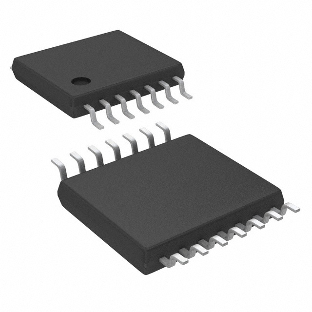
- Part No.:
- MAX9202EUD+
- Manufacturer:
- Analog Devices Inc./Maxim Integrated
- Category:
- Comparators
- Package:
- 14-TSSOP (0.173", 4.40mm Width)
- Datasheet:
-
 MAX9202EUD+.pdf
- Description:
- IC COMPARATOR 2 W/LATCH 14TSSOP
- Quantity:
- Payment:

- Shipping:

Inventory:106
Please send an inquiry. Send us your inquiry, and we will respond immediately.
Product details
Overview
The MAX9202EUD+ from Maxim Integrated is a dual high-speed voltage comparator with TTL-compatible outputs and latch inputs, designed for precision timing-critical signal discrimination in mixed-signal systems. It delivers 7ns typical propagation delay (at 5mV overdrive), 9mW per comparator power consumption at +5V supply, and supports separate analog (±5V or +5V to +10V) and digital (+5V) supplies. It is used in high-speed A/D converters, line receivers, and PWM circuits where fast, low-power threshold detection with output hold capability is required.
For engineers reviewing the MAX9202EUD+ datasheet, MAX9202EUD+ pinout, MAX9202EUD+ application, or MAX9202EUD+ equivalent, this page provides verified functional specifications, validated dual-comparator timing behavior, confirmed TSSOP-14 package mapping, and real-world design context for signal restoration and sampling applications requiring latch-controlled output capture.
Technical Context
The MAX9202EUD+ integrates two independent comparators with internal TTL pullups and dedicated latch control inputs (LATCHA, LATCHB) that freeze output states on logic-low assertion. Its bipolar process enables rail-to-rail common-mode input range down to VEE (–5V), supporting ground-sensing operation with single +5V supply when VEE = GND.
Propagation delay is tightly matched between channels (∆tPD ≤ 2.5ns over temperature), and timing parameters-including tPD+(D) and tPD–(D) ≤ 10ns-guarantee deterministic latch-release response. Input offset voltage remains ≤ 7.5mV across –40°C to +85°C, ensuring stable threshold accuracy in industrial environments.
Key Specifications
| Parameter | Value and Actual Design Meaning |
|---|---|
| Propagation Delay | 7ns typical (5mV overdrive); enables sub-10ns decision latency in high-speed sampling circuits. |
| Power per Comparator | 9mW at +5V supply; reduces thermal load and simplifies power budgeting in dense PCB layouts. |
| Analog Supply Range | +5V to +10V (VEE = GND) or ±5V; supports flexible system-level power architecture without level-shifting. |
| Input Common-Mode Range | VEE – 0.1V to VCC – 2.25V; allows direct sensing of signals referenced to negative rails or ground. |
| Output Drive Capability | VOH ≥ 3.0V @ 1mA sink, VOL ≤ 0.4V @ 8mA source; ensures robust TTL fan-out of four. |
| Latch Timing | tS = 2ns setup, tN = 1ns hold, tPW(D) = 8ns minimum pulse width; enables reliable capture in nanosecond-scale control windows. |
Pinout & Package
MAX9202EUD+ is housed in a 14-pin TSSOP package (JEDEC MO-153, 5.0mm × 4.4mm × 1.2mm), optimized for high-density mixed-signal PCBs with thermal and EMI performance advantages over SOIC.
| Pin/Terminal | Circuit Role | Design Meaning |
|---|---|---|
| 1, 8 | IN_– (A, B) | Negative input terminals for comparator channels A and B; accept differential or single-ended signals down to VEE. |
| 2, 9 | IN_+ (A, B) | Positive input terminals for channels A and B; support rail-to-rail common-mode range with <4pF input capacitance. |
| 3 | GND | Digital ground reference for VDD and latch inputs; must be isolated from analog ground (VEE) in split-supply configurations. |
| 4, 11 | LATCH_ (A, B) | TTL-compatible latch enable inputs; low-level assertion freezes respective comparator output state until next high-to-low transition. |
| 5, 12 | OUT_ (A, B) | TTL-output terminals with active internal pullups; drive standard LS-TTL loads without external resistors. |
| 6, 13 | N.C. | No internal connection; must remain unconnected and unbonded per Maxim design. |
| 7 | VEE | Negative analog supply and substrate bias; sets lower bound of input common-mode range and must be decoupled locally. |
| 10 | VDD | +5V digital supply for latch circuitry and output stage; requires dedicated 100nF ceramic decoupling capacitor. |
| 14 | VCC | Positive analog supply (4.75V–10.5V); powers comparator core and determines input dynamic range and speed. |
Key Features
| Feature | Design Value |
|---|---|
| Dual-channel latch control | Independent LATCHA/LATCHB inputs allow asynchronous capture of two signal thresholds without shared timing constraints. |
| Rail-inclusive input range | Common-mode range extends to VEE – 0.1V, enabling direct interface with sensors or DACs operating near negative supply rails. |
| Matched channel timing | ∆tPD ≤ 2.5ns ensures synchronized decision latency between channels-critical for phase-sensitive applications like encoder decoding. |
| Low-power bipolar architecture | 9mW/comparator at +5V reflects optimized transistor count (176) and eliminates need for external bias networks or power sequencing. |
| TTL output integration | Internal pullups eliminate external resistors while maintaining full LS-TTL compatibility (fan-out of four) and reducing BOM count. |
Applications
| High-Speed A/D Converters | Line Receivers |
|---|---|
|
Use Scenario: Sampling analog input at >100 MSPS using flash or pipeline ADC architectures where comparator decisions define conversion windows. IC Role / Device Role / Timing Role: Dual comparator acts as front-end threshold detector and clock-synchronized sample gate, with latches capturing instantaneous analog levels prior to quantization. Use Value: 7ns propagation delay and 2ns setup time ensure minimal aperture jitter (<1ps RMS contribution), preserving effective resolution in 12-bit+ systems. |
Use Scenario: Receiving differential or single-ended data streams over twisted-pair or coaxial cables in industrial fieldbus or test equipment interfaces. IC Role / Device Role / Timing Role: Comparator functions as high-speed line receiver with hysteresis-free decision making; latch holds valid data during clock domain crossing or bus arbitration. Use Value: Rail-to-rail input range and TTL output drive directly interface with FPGA I/O banks or microcontroller GPIOs without level shifters or external buffers. |
| PWM Signal Conditioning | Threshold Detectors |
|
Use Scenario: Monitoring motor phase currents or switching node voltages in real-time to trigger fault shutdown or adaptive dead-time control. IC Role / Device Role / Timing Role: Dual comparator compares sensed current/voltage against programmable thresholds; latches capture peak or zero-crossing events for deterministic interrupt generation. Use Value: Matched channel delay (≤2.5ns skew) ensures simultaneous evaluation of complementary PWM edges, preventing false overcurrent triggers in three-phase inverters. |
Use Scenario: Detecting precise voltage thresholds in battery management, power supply supervision, or sensor alarm circuits. IC Role / Device Role / Timing Role: Comparator serves as ultra-fast window or level detector; latch holds alarm state until host MCU reads and clears condition. Use Value: 7.5mV max input offset and 250µV/V CMRR maintain threshold accuracy across temperature and supply variation-critical for <1% tolerance monitoring. |
Equivalent & Alternatives
The following parts are listed as comparable options for similar dual high-speed comparator with latch applications.
| Alternative Part | Technical Difference | Application Difference | Selection Advice |
|---|---|---|---|
| MAX9202EUD | Same die, identical electrical specs and pinout; differs only in tape-and-reel packaging and RoHS compliance (EUD+ includes lead-free finish and green marking). | No functional difference; EUD+ replaces EUD in new designs requiring RoHS-6 compliance and JEDEC-standard moisture sensitivity level (MSL3). | Select MAX9202EUD+ for production builds requiring RoHS compliance, traceability, and extended shelf-life handling per J-STD-020. |
| LM393DR | Single comparator, no latch, 1.3µs propagation delay, 0.8mW power; lacks dual-channel timing match, TTL latch interface, and rail-inclusive input range. | Suitable only for non-critical, low-speed threshold detection (e.g., battery low-voltage warning); cannot replace MAX9202EUD+ in latch-dependent or high-speed sampling roles. | Use LM393DR only in cost-sensitive, low-frequency applications where 7ns timing, latch control, and dual-channel synchronization are unnecessary. |
Compared with MAX9202EUD+, the MAX9202EUD offers identical functionality but lacks RoHS-6 compliance and MSL3 qualification, while the LM393DR falls short in speed, channel count, latch capability, and input range-making it unsuitable for any application requiring the precise timing or dual-latched behavior of the MAX9202EUD+.
Availability
MAX9202EUD+ is available at Aetrix Electronics and suitable for high-speed A/D converters, line receivers, and PWM signal conditioning requiring stable component supply, long-term lifecycle assurance, and RoHS-compliant manufacturing.
Supply support for MAX9202EUD+ includes scheduled delivery planning, volume procurement assistance, BOM continuity management, traceable sourcing, and lifecycle availability coordination for OEM customers, industrial embedded developers, connected-device designers, and electronics production programs.
Manufacturer
Maxim Integrated (now part of Analog Devices) is a U.S.-based semiconductor company specializing in high-performance analog, mixed-signal, and RF solutions for industrial, communications, and computing markets.
The MAX9202EUD+ belongs to Maxim's low-power, high-speed comparator product line, engineered specifically for applications demanding sub-10ns decision latency, latch-controlled output capture, and flexible multi-supply operation in space-constrained industrial systems.
FAQ
What is the maximum operating temperature range for the MAX9202EUD+?
The MAX9202EUD+ is specified for continuous operation from –40°C to +85°C. This industrial-grade temperature range is fully guaranteed by design and verified across all electrical parameters including propagation delay, input offset voltage, and latch timing. The device's junction temperature limit is +150°C, allowing margin for transient thermal excursions in high-density PCB layouts. All production units undergo 100% testing at +25°C, with design validation covering the full –40°C to +85°C range.
Does the MAX9202EUD+ support single-supply operation?
Yes, the MAX9202EUD+ supports true single-supply operation with VEE tied to ground and VCC set between +5V and +10V. In this configuration, its analog input common-mode range extends from 0V (GND) to VCC – 2.25V, enabling ground-referenced signal sensing. The digital supply VDD remains fixed at +5V. This mode is explicitly validated in the datasheet's "Typical Power-Supply Alternatives" section (Figure 1b) and confirmed in the Absolute Maximum Ratings table.
What is the function of pins 6 and 13 on the MAX9202EUD+?
Pins 6 and 13 on the MAX9202EUD+ are marked N.C. (No Connection) in the official pin description table and must remain unconnected. These pins have no internal bond wire or circuit connection and serve only as mechanical alignment aids in the TSSOP-14 package. Connecting them to any voltage or ground violates Maxim's recommended layout guidelines and may cause unpredictable behavior due to parasitic coupling or package stress effects.
How does the latch feature work on the MAX9202EUD+?
The MAX9202EUD+ features two independent TTL-compatible latch inputs (LATCHA on pin 4, LATCHB on pin 11). When either input is driven low, the corresponding comparator output freezes in its current logic state and ignores further input transitions until the latch input returns high. The latch release timing is characterized as tPD+(D) ≤ 10ns and tPD–(D) ≤ 10ns. This behavior is confirmed in the Timing Characteristics table and Applications Information section, and applies only to the MAX9202/MAX9203-not the MAX9201.
What decoupling capacitors are recommended for the MAX9202EUD+?
Maxim specifies 100nF ceramic capacitors placed as close as possible to each power pin: one between VCC and VEE, one between VDD and GND, and optionally a second 100nF cap between VCC and GND if VEE = GND in single-supply mode. These values are derived from the "Circuit Layout" section, which emphasizes low-inductance grounding and minimizes trace length to suppress high-frequency noise coupling into the comparator's sensitive analog inputs. Larger bulk capacitors (e.g., 1µF tantalum) are not required per datasheet guidance.
MAX9202EUD+ Specifications
- Product attributes
- Attribute value
- Manufacturer:
- Analog Devices Inc./Maxim Integrated
- Package/Case:
- 14-TSSOP (0.173", 4.40mm Width)
- Series:
- -
- Packaging:
- Tube
- Product Status:
- Active
- Type:
- with Latch
- Number of Elements:
- 2
- Output Type:
- TTL
- Voltage - Supply, Single/Dual (±):
- 4.75V ~ 10.5V, ±2.375V ~ 5.75V
- :
- 4mV @ ±5V
- Voltage - Input Offset (Max):
- 5µA @ ±5V
- Current - Input Bias (Max):
- -
- Current - Output (Typ):
- 4mA, 3mA, 1.5mA
- Current - Quiescent (Max):
- 86.02dB CMRR, 86.02dB PSRR
- CMRR, PSRR (Typ):
- -
- Propagation Delay (Max):
- -
- Hysteresis:
- -40°C ~ 85°C
- Operating Temperature:
- -
- Grade:
- -
- Qualification:
- Surface Mount
- :
- 14-TSSOP
MAX9202EUD+ FAQ
1.How can I place an order for MAX9202EUD+ through Aetrix?
Please submit a Request for Quotation (RFQ) for MAX9202EUD+ on Aetrix. Our sales agent will provide a competitive quotation and guide you through the order confirmation once you accept the terms.
2.Are the price and stock information for MAX9202EUD+ reliable?
The price and inventory of MAX9202EUD+ are updated periodically and may fluctuate due to market conditions. Stock and pricing data are typically refreshed every 24 hours. Quotation validity for MAX9202EUD+ is usually 5 days.
3.What payment methods are accepted for MAX9202EUD+?
We accept Wire Transfer, PayPal, Credit Card, Western Union, MoneyGram, and Escrow for MAX9202EUD+ transactions.
Note: Certain payment methods may incur a processing fee.
4.How is shipping managed for MAX9202EUD+?
MAX9202EUD+ orders can be shipped via leading logistics carriers, including DHL, UPS, FedEx, TNT, or Registered Mail.
Once your MAX9202EUD+ order is processed, you will receive an email with the shipment details and tracking number.
Note: Tracking information may take up to 24 hours to appear. Express delivery typically takes 3–5 business days.
5.How can I obtain technical support or documentation for MAX9202EUD+?
For technical support, including MAX9202EUD+ datasheets, pinout diagrams, or application guidance, please contact our engineering support team. They can provide detailed documentation and assistance for your MAX9202EUD+ requirements.
6.How does Aetrix verify that MAX9202EUD+ is sourced from the original manufacturer or authorized distributors?
All MAX9202EUD+ products on Aetrix are procured from qualified distributors and authorized channels. Our dedicated quality assurance team conducts strict verification, including traceability checks and, if necessary, third-party testing. This ensures that MAX9202EUD+ meets industry standards.
7.What is the process for return or replacement of MAX9202EUD+?
All MAX9202EUD+ units undergo pre-shipment inspection (PSI). If there is an issue with MAX9202EUD+, returns or replacements are accepted under the following conditions:
1.Quantity discrepancies, incorrect items, or visible external defects (such as breakage or corrosion), acknowledged by Aetrix.
2.The issue is reported within 90 days of delivery.
3.The MAX9202EUD+ part is unused and in its original packaging.
Return procedure for MAX9202EUD+:
1.Submit a request within 90 days.
2.Obtain a Return Material Authorization (RMA) from Aetrix.
MAX9202EUD+ Tags

-
LM2903DR
Texas Instruments

-
LM339DR
Texas Instruments

-
LM339PWR
Texas Instruments

-
LM393DT
STMicroelectronics
-
LM2901PWR
Texas Instruments
-
LM2903DT
STMicroelectronics
-
LM393DR
Texas Instruments
-
LM239DR
Texas Instruments
-
LM339APWR
Texas Instruments

-
LM2903P
Texas Instruments
-
LM393ADR
Texas Instruments
-
NCX2200GMAZ
NXP USA Inc.
Tech Hub

An engineering guide to LED driver operation, constant-current and constant-voltage outputs, linear and switching topologies, dimming, IC selection, calculations, replacement compatibility, and fault c…

Operational amplifier guide covering op amp basics, feedback, ideal vs real op amps, common configurations, buffer circuits, offset, bias current, gain-bandwidth, slew rate, rail-to-rail limits and sel…

Jumper cables guide covering safe connection order, red and black clamp placement, final ground connection, cable gauge, length, clamp quality, copper vs CCA cables, jump starter comparison and battery…

LDO regulator guide covering low dropout voltage, power dissipation, thermal design, PSRR, output noise, capacitor stability, adjustable LDO circuits, LDO vs buck converter and datasheet selection chec…

Conditional Access Module guide covering CAM meaning, CI/CI+ interface, smart card authorization, DVB security workflow, TV and set-top box compatibility, internal electronics, ESD protection, connecto…

Guide to electronic component obsolescence covering EOL risk, PCN/PDN notices, last-time buy planning, replacement options, form-fit-function validation, counterfeit risk and BOM lifecycle management.

18650 battery guide covering lithium-ion cell basics, 3.6V/3.7V voltage, 4.2V charging, mAh and Wh capacity, protected cells, chargers, BMS, series-parallel packs, holders, welding and sourcing checks.…

Hall effect sensor guide covering working principle, linear and digital sensors, Arduino circuits, current sensing, speed detection, automotive applications, A3144 examples, signal filtering and datash…

Product Change Notification guide for electronic components, covering PCN meaning, PCN vs PDN/EOL, common change types, risk levels, form-fit-function review, engineering validation, BOM control, LTB/L…

A practical guide to blend door actuators, covering HVAC function, symptoms, location, AC and heater issues, reset and calibration, replacement cost, electrical diagnosis, compatibility checks, and rep…


