
 My Inquiry
 My Account


Analog Devices Inc./Maxim Integrated MAX9218ECM+T
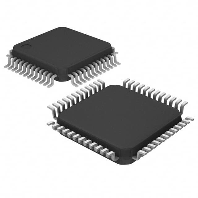
- Part No.:
- MAX9218ECM+T
- Manufacturer:
- Analog Devices Inc./Maxim Integrated
- Category:
- Serializers, Deserializers
- Package:
- 48-LQFP
- Datasheet:
-
 MAX9218ECM+T.pdf
- Description:
- IC DESERIALIZER LVDS 48-LQFP
- Quantity:
- Payment:

- Shipping:

Inventory:911
Please send an inquiry. Send us your inquiry, and we will respond immediately.
Product details
Overview
The MAX9218ECM+T from Maxim Integrated is a 27-bit, DC-balanced LVDS deserializer IC that converts high-speed serial video and control data into parallel RGB (18-bit) and control (9-bit) outputs. It operates at 7MHz–35MHz parallel clock rates, supports AC-coupled LVDS links, features selectable rising/falling output latch edge, and pairs with the MAX9217 serializer for automotive display interfaces.
For engineers reviewing the MAX9218ECM+T datasheet, MAX9218ECM+T pinout, MAX9218ECM+T application, or MAX9218ECM+T equivalent, this page delivers verified electrical specs, validated LQFP-48 pin mapping, confirmed ESD ratings (±10kV contact), dual-supply operation (+3.3V core / 1.8V–3.3V VCCO), and real-world timing behavior including PCLK_OUT stretch on lock and DE_OUT-driven phase switching.
Technical Context
The MAX9218ECM+T implements a proprietary DC-balanced encoding/decoding scheme to enable AC coupling and reduce EMI across long cables. Its PLL synchronizes first to REFCLK (±2% tolerance), then locks to the recovered serial clock - with lock time up to 16,385 REFCLK cycles - before enabling valid RGB_OUT[17:0] and CNTL_OUT[8:0] outputs.
It separates video and control phases using DE_OUT signaling: video data appears on RGB_OUT[17:0] during active video (DE_OUT = high), while 9-bit control data appears on CNTL_OUT[8:0] during blanking (DE_OUT = low). Five control bits (C0–C4) use majority voting for single-bit error tolerance; C5–C8 are direct-pass.
Key Specifications
| Parameter | Value and Actual Design Meaning |
|---|---|
| Parallel Clock Range | 7MHz to 35MHz - defines minimum/maximum pixel clock rate supported for RGB video timing |
| Serial Data Rate | 140Mbps to 700Mbps - scales with clock range (15–35MHz → 300–700Mbps); enables CAT5e cable runs ≤12m at BER <10⁻¹² |
| Output Supply Range (VCCO) | 1.8V to 3.3V - allows direct interfacing to 1.8V, 2.5V, or 3.3V logic without level shifters |
| Core Supply Voltage | +3.3V (±10%) - powers digital core and LVTTL/LVCMOS inputs; requires local 0.1µF + 0.001µF bypassing |
| ESD Protection | ±10kV contact / ±30kV air (ISO 10605) - certified for harsh automotive environments with no external protection needed |
| Operating Temperature | -40°C to +85°C - qualified for under-hood and display module applications in passenger vehicles |
| Input Reference Tolerance | ±2% - permits use of low-cost crystal oscillators instead of TCXOs for REFCLK input |
Pinout & Package
MAX9218ECM+T is packaged in a 48-lead LQFP (Lead-Free, RoHS-compliant) with exposed pad (not electrically connected). Pin functions are fully defined per Maxim's official pin description table and functional diagram.
| Pin/Terminal | Circuit Role | Design Meaning |
|---|---|---|
| R/F | Latch edge select input | Configures PCLK_OUT edge (rising/falling) for latching RGB_OUT/CNTL_OUT into downstream logic |
| RNG1, RNG0 | Frequency range select inputs | Set operating band (7–15MHz or 15–35MHz) and corresponding output transition time (slow/fast) |
| IN+, IN- | Differential LVDS serial input | Accepts DC-balanced 700Mbps serial stream; internally biased to 1.2V for AC-coupled operation |
| REFCLK | Reference clock input | Provides initial PLL reference; must be within ±2% of serializer PCLK_IN frequency |
| PWRDWN | Power-down control | Drives all outputs to high-Z and stops PLL when ≤0.3V; reduces ICC to <50µA |
| OUTEN | Output enable | Enables/disables all single-ended outputs (RGB_OUT, CNTL_OUT, DE_OUT, PCLK_OUT, LOCK) |
| DE_OUT | Data enable output | High = RGB_OUT[17:0] valid; Low = CNTL_OUT[8:0] valid - enables time-multiplexed bus sharing |
| RGB_OUT[17:0] | Parallel video data outputs | 18-bit RGB video bus (RGB_OUT0–RGB_OUT17); grouped into staggered 6-bit banks to reduce ground bounce |
| CNTL_OUT[8:0] | Parallel control data outputs | 9-bit control bus (CNTL_OUT0–CNTL_OUT8); C0–C4 tolerate single-bit errors via majority voting |
| PCLK_OUT | Recovered parallel clock output | Stretches during lock transition; drives downstream latch edge synchronized to serialized data |
| LOCK | Lock status indicator | Low = valid synchronized outputs; High = loss of lock or initialization - used for system fault detection |
| VCC, VCCO, VCCLVDS, VCCPLL | Independent supply rails | Four isolated power domains prevent noise coupling between digital, output, LVDS, and PLL sections |
Key Features
| Feature | Design Value |
|---|---|
| Proprietary DC-balanced decoding | Enables AC coupling with standard 0.1µF capacitors; eliminates DC offset drift and common-mode noise accumulation over long cables |
| Video/control phase separation | Uses DE_OUT to time-multiplex 18-bit RGB video and 9-bit control data on same physical interface - avoids dedicated control lines and saves PCB routing |
| Staggered RGB output switching | Groups RGB_OUT[17:0] into three 6-bit banks switching ~1ns apart - cuts peak current demand and reduces simultaneous switching noise (SSN) |
| Selectable output transition time | RNG[1:0] configures fast/slow slew rates (3.2–5.5ns rise/fall) to optimize EMI vs. timing margin trade-off per clock frequency band |
| Single-bit error tolerance (C0–C4) | Majority voting across three repeated bits ensures robust control channel operation in noisy automotive EMI environments |
| Separate VCCO supply | Allows direct connection to 1.8V/2.5V/3.3V logic families without external level translators - simplifies interface design and reduces BOM count |
Applications
| Navigation System Display | In-Vehicle Entertainment System |
|---|---|
Use Scenario: High-resolution TFT-LCD display in center-stack infotainment unit receiving video from camera or media processor over 1–3m harness. IC Role / Device Role / Timing Role: Deserializes LVDS video stream into parallel RGB and control signals; provides DE_OUT-synchronized timing for display controller latch alignment. Use Value: Enables compact, EMI-robust cabling using cost-effective CAT5e; AC coupling isolates display module ground from head-unit ground, eliminating ground-loop artifacts. |
Use Scenario: Rear-seat entertainment display receiving HDMI video converted to LVDS via MAX9217 serializer at source. IC Role / Device Role / Timing Role: Recovers pixel clock and video data; uses CNTL_OUT[8:0] to pass touch-panel commands or backlight dimming signals back to source. Use Value: Dual-phase operation eliminates need for separate I²C/SPI control bus; single cable carries both video and bidirectional control traffic. |
| Video Camera Interface | LCD Displays |
Use Scenario: Front/rear camera module transmitting raw video to ADAS domain controller over shielded twisted-pair cable. IC Role / Device Role / Timing Role: Converts serialized camera sensor output into parallel RGB for image processing; LOCK signal validates data integrity before frame capture. Use Value: ±10kV ISO 10605 ESD rating protects against handling damage during assembly; wide temperature range ensures reliability in engine-bay-mounted cameras. |
Use Scenario: Industrial or automotive LCD panel requiring precise RGB timing and brightness control via embedded microcontroller. IC Role / Device Role / Timing Role: Provides synchronous RGB_OUT[17:0] and PCLK_OUT to drive display timing controller; CNTL_OUT[8:0] delivers gamma correction or power sequencing commands. Use Value: Output enable (OUTEN) allows busing multiple MAX9218 outputs to shared display bus - reducing pin count on host MCU and simplifying layout. |
Equivalent & Alternatives
The following parts are listed as comparable options for similar LVDS deserializer applications.
| Alternative Part | Technical Difference | Application Difference | Selection Advice |
|---|---|---|---|
| MAX9248GTJ+T | Higher speed (up to 100MHz parallel clock), 24-bit RGB + 3-bit control, integrated FPD-Link III decoder | Targets next-gen displays with higher resolution and embedded control protocols (e.g., MIPI DSI bridging) | Choose MAX9248GTJ+T only if migrating to FPD-Link III infrastructure; not drop-in compatible due to different protocol stack and pinout |
| TI DS90UB925QSQ/NOPB | Fully pin-compatible with MAX9218 in 48-pin QFN; identical 27-bit deserialization, but uses FPD-Link II protocol and lacks DE_OUT multiplexing | Requires external control bus (I²C) for configuration; no native control-data phase multiplexing | Valid alternative for legacy FPD-Link II systems where control data is handled separately; verify REFCLK tolerance (±1%) and ESD rating (±8kV) match system requirements |
Compared with MAX9218ECM+T, MAX9248GTJ+T offers higher bandwidth and protocol flexibility but demands redesign; DS90UB925QSQ/NOPB provides mechanical compatibility and similar performance but removes the DE_OUT-based video/control time-division feature critical for space-constrained automotive displays.
Availability
MAX9218ECM+T is available at Aetrix Electronics and suitable for automotive navigation systems, in-vehicle entertainment modules, camera interface designs, and industrial LCD displays requiring stable component supply across extended temperature ranges and long production lifecycles.
Supply support for MAX9218ECM+T includes scheduled delivery planning, volume procurement assistance, BOM continuity management, traceable sourcing, and lifecycle availability coordination for OEM customers, industrial embedded developers, connected-device designers, and electronics production programs.
Manufacturer
Maxim Integrated (now part of Analog Devices) designs precision analog, mixed-signal, and high-speed interface ICs for automotive, industrial, and communications markets.
The MAX9218ECM+T belongs to Maxim's automotive-grade LVDS serializer/deserializer family, engineered specifically for noise-immune, long-cable video transmission in safety-critical display and camera systems.
FAQ
What is the maximum cable length supported by MAX9218ECM+T at 35MHz?
The MAX9218ECM+T supports up to 12 meters of CAT5e cable at 35MHz (700Mbps) with bit-error rate <10⁻¹², as verified in Maxim's typical operating characteristics. Performance depends on cable quality, termination, and noise environment; shorter lengths (≤5m) are recommended for worst-case EMI conditions in engine compartments.
Does MAX9218ECM+T require an external oscillator for REFCLK?
Yes, MAX9218ECM+T requires an external LVTTL/LVCMOS reference clock applied to the REFCLK pin. The device accepts frequencies from 7MHz to 35MHz with ±2% tolerance - allowing use of low-cost crystals or oscillators without tight stability specs. No internal oscillator is present.
How does the MAX9218ECM+T handle loss of serial input signal?
When the LVDS input stops switching, MAX9218ECM+T drives LOCK high, sets all outputs (except PCLK_OUT) low, and routes REFCLK to PCLK_OUT. This fail-safe state alerts the system to link failure while maintaining clock continuity for diagnostics - critical for ASIL-B compliant display monitoring.
Can MAX9218ECM+T interface directly with a 1.8V FPGA I/O bank?
Yes, MAX9218ECM+T supports 1.8V logic levels via its independent VCCO supply. Set VCCO = 1.8V, and RGB_OUT[17:0], CNTL_OUT[8:0], DE_OUT, PCLK_OUT, and LOCK will swing rail-to-rail between 0V and 1.8V - eliminating level shifters and reducing board area and power consumption.
What is the purpose of the RNG0 and RNG1 pins on MAX9218ECM+T?
RNG0 and RNG1 configure the MAX9218ECM+T's operating frequency band and output transition time: 01 selects 7–15MHz (slow slew), 11 selects 15–35MHz (fast slew). Incorrect settings cause timing violations or excessive EMI - they must match the MAX9217 serializer's PCLK_IN frequency.
MAX9218ECM+T Specifications
- Product attributes
- Attribute value
- Manufacturer:
- Analog Devices Inc./Maxim Integrated
- Series:
- -
- Package/Case:
- 48-LQFP
- Packaging:
- Tape & Reel (TR)
- Product Status:
- Active
- Function:
- Deserializer
- Data Rate:
- 700Mbps
- Input Type:
- LVDS
- Output Type:
- LVCMOS, LVTTL
- Number of Inputs:
- 1
- Number of Outputs:
- 27
- Voltage - Supply:
- 3V ~ 3.6V
- Operating Temperature:
- -40°C ~ 85°C (TA)
- Grade:
- -
- Qualification:
- -
- Mounting Type:
- Surface Mount
- Supplier Device Package:
- 48-LQFP (7x7)
MAX9218ECM+T FAQ
1.How can I place an order for MAX9218ECM+T through Aetrix?
Please submit a Request for Quotation (RFQ) for MAX9218ECM+T on Aetrix. Our sales agent will provide a competitive quotation and guide you through the order confirmation once you accept the terms.
2.Are the price and stock information for MAX9218ECM+T reliable?
The price and inventory of MAX9218ECM+T are updated periodically and may fluctuate due to market conditions. Stock and pricing data are typically refreshed every 24 hours. Quotation validity for MAX9218ECM+T is usually 5 days.
3.What payment methods are accepted for MAX9218ECM+T?
We accept Wire Transfer, PayPal, Credit Card, Western Union, MoneyGram, and Escrow for MAX9218ECM+T transactions.
Note: Certain payment methods may incur a processing fee.
4.How is shipping managed for MAX9218ECM+T?
MAX9218ECM+T orders can be shipped via leading logistics carriers, including DHL, UPS, FedEx, TNT, or Registered Mail.
Once your MAX9218ECM+T order is processed, you will receive an email with the shipment details and tracking number.
Note: Tracking information may take up to 24 hours to appear. Express delivery typically takes 3–5 business days.
5.How can I obtain technical support or documentation for MAX9218ECM+T?
For technical support, including MAX9218ECM+T datasheets, pinout diagrams, or application guidance, please contact our engineering support team. They can provide detailed documentation and assistance for your MAX9218ECM+T requirements.
6.How does Aetrix verify that MAX9218ECM+T is sourced from the original manufacturer or authorized distributors?
All MAX9218ECM+T products on Aetrix are procured from qualified distributors and authorized channels. Our dedicated quality assurance team conducts strict verification, including traceability checks and, if necessary, third-party testing. This ensures that MAX9218ECM+T meets industry standards.
7.What is the process for return or replacement of MAX9218ECM+T?
All MAX9218ECM+T units undergo pre-shipment inspection (PSI). If there is an issue with MAX9218ECM+T, returns or replacements are accepted under the following conditions:
1.Quantity discrepancies, incorrect items, or visible external defects (such as breakage or corrosion), acknowledged by Aetrix.
2.The issue is reported within 90 days of delivery.
3.The MAX9218ECM+T part is unused and in its original packaging.
Return procedure for MAX9218ECM+T:
1.Submit a request within 90 days.
2.Obtain a Return Material Authorization (RMA) from Aetrix.
MAX9218ECM+T Tags

-
SN65HVS880PWPR
Texas Instruments
-
SN65HVS882PWPR
Texas Instruments

-
FIN3386MTDX
onsemi
-
FIN3385MTDX
onsemi

-
SN65LV1023ARHBR
Texas Instruments

-
SN65LV1023ADBR
Texas Instruments
-
SN65LV1224BDBR
Texas Instruments

-
SN65LVDS93ADGGR
Texas Instruments
-
SN65LVDS93DGGR
Texas Instruments

-
TDES954RGZT
Texas Instruments
-
SN65LV1224BRHBT
Texas Instruments

-
DS90UB914QSQE/NOPB
Texas Instruments
Tech Hub

A practical engineering guide to 3.3V and 5V logic compatibility, input thresholds, resistor dividers, translator ICs, MOSFET level shifting, I2C pull-ups, timing limits and power-sequencing risks.

The 74HC595 uses push-pull logic outputs, while the TPIC6B595 uses 50 V open-drain DMOS sinks for higher-power loads. This guide compares timing, current limits, 3.3 V interfacing, load wiring, thermal…

The 74HC595 converts serial data into eight stable parallel outputs. This guide covers pin functions, shift and storage timing, OE and MR behavior, drive-current limits, cascading, voltage compatibilit…

A technical comparison of level-sensitive latches and edge-triggered flip-flops, covering timing windows, setup and hold limits, master–slave operation, time borrowing, race-through, HDL inference and…

A D latch stores one bit while Enable controls when data can pass. This reference covers gate-level operation, truth tables, transparency, setup and hold timing, LE versus OE, common ICs and practical …

An SR latch stores one bit through cross-coupled feedback. This engineering reference covers NOR and NAND implementations, truth tables, forbidden-state recovery, gated operation, switch debouncing, fa…

Latch circuits retain one bit through feedback. This technical reference covers SR and D latches, truth tables, transparency, timing limits, latch-versus-flip-flop behavior, applications and common log…

An engineering guide to LED driver operation, constant-current and constant-voltage outputs, linear and switching topologies, dimming, IC selection, calculations, replacement compatibility, and fault c…

Operational amplifier guide covering op amp basics, feedback, ideal vs real op amps, common configurations, buffer circuits, offset, bias current, gain-bandwidth, slew rate, rail-to-rail limits and sel…

Jumper cables guide covering safe connection order, red and black clamp placement, final ground connection, cable gauge, length, clamp quality, copper vs CCA cables, jump starter comparison and battery…


