
 My Inquiry
 My Account


Analog Devices Inc./Maxim Integrated MAX9248ETM+
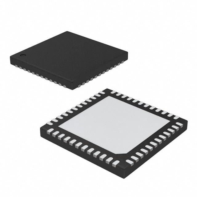
- Part No.:
- MAX9248ETM+
- Manufacturer:
- Analog Devices Inc./Maxim Integrated
- Category:
- Serializers, Deserializers
- Package:
- 48-WFQFN Exposed Pad
- Datasheet:
-
 MAX9248ETM+.pdf
- Description:
- IC DESERIALIZER LVDS 48-TQFN
- Quantity:
- Payment:

- Shipping:

Inventory:3,975
Please send an inquiry. Send us your inquiry, and we will respond immediately.
Product details
Overview
MAX9248ETM+ from Maxim Integrated is a 27-bit DC-balanced LVDS deserializer IC that converts high-speed serial video/control data into 18-bit RGB video and 9-bit control parallel outputs. It operates at 5MHz–42MHz parallel clock frequency, features ±2% or ±4% programmable spread-spectrum output for EMI reduction, and interfaces with MAX9247 serializer in automotive display systems.
For engineers reviewing the MAX9248ETM+ datasheet, MAX9248ETM+ pinout, MAX9248ETM+ application, or MAX9248ETM+ equivalent, this page delivers verified technical context, real-world timing behavior, latch-edge configuration options, spread-spectrum modulation impact on system-level EMI, and validated alternatives for in-vehicle infotainment video links.
Technical Context
The MAX9248ETM+ implements a dual-phase deserialization architecture: video data (RGB_OUT[17:0]) is latched during DE_OUT high periods, while control data (CNTL_OUT[8:0]) is recovered during DE_OUT low periods-leveraging video blanking intervals to reduce required serial bandwidth. Its proprietary DC-balanced encoding enables AC-coupling across long cables without common-mode drift.
It integrates two PLLs: a reference-lock PLL synchronizing to REFCLK (±2% tolerance), and a spread-spectrum PLL (SSPLL) modulating PCLK_OUT and data outputs at 32kHz base rate (scaling linearly with input clock). Input-to-output delay ranges from (4.5tT + 8.0)ns to (36tT + 16)ns due to SSPLL variation, with lock time up to 33,600 REFCLK cycles.
Key Specifications
| Parameter | Value and Actual Design Meaning |
|---|---|
| Deserialization Width | 27-bit total: 18-bit RGB video + 9-bit control data, separated by DE_OUT state-enables efficient use of video blanking for control channel. |
| Parallel Clock Range | 5MHz to 42MHz; supports CAT5 cable runs up to 12m at 42MHz with BER < 10⁻¹²-validated for automotive display pixel clocks. |
| Spread-Spectrum Control | SS input selects ±2% (low) or ±4% (high) frequency deviation around REFCLK; reduces peak EMI by >10dB in 100kHz RBW measurements. |
| Input Sensitivity | LVDS differential threshold ±50mV; supports 0.05V–1.2V VID range and internal 42kΩ–78kΩ bias resistors-enables robust operation with AC-coupled 100Ω STP links. |
| Output Supply Flexibility | VCCO supports 1.8V–3.3V logic levels; allows direct interfacing to FPGA I/O banks or ASIC video processors without level shifters. |
| ESD Robustness | ±10kV contact / ±30kV air-gap per ISO 10605; meets automotive EMC requirements for display interface ICs in harsh environments. |
| Operating Temperature | -40°C to +105°C; qualified for under-hood and center-stack display applications per AEC-Q100 stress test profiles. |
Pinout & Package
MAX9248ETM+ is housed in a 48-lead LQFP package (7mm × 7mm, 0.5mm pitch) with exposed thermal pad. Pin functions are electrically and physically distinct between MAX9248 and MAX9250 variants; this part uses SS (not OUTEN) and lacks output enable functionality.
| Pin/Terminal | Circuit Role | Design Meaning |
|---|---|---|
| R/F | Latch edge select | Configures PCLK_OUT edge (rising/falling) for latching RGB_OUT/CNTL_OUT into downstream logic-critical for timing closure with FPGAs or display controllers. |
| SS | Spread-spectrum enable | High = ±4% output frequency spread; low = ±2%-directly controls EMI profile without firmware or register writes. |
| REFCLK | Reference clock input | Local 5MHz–42MHz clock source used for initial PLL lock before serial link acquisition; ±2% tolerance allows low-cost crystal oscillators. |
| IN+/IN- | LVDS serial input pair | Differential receiver for 840Mbps max serial stream from MAX9247; internally biased to 1.2V for AC-coupled operation. |
| RGB_OUT[17:0] | Video data outputs | Three staggered 6-bit groups reduce simultaneous switching noise; each group transitions ~1ns apart to minimize ground bounce. |
| CNTL_OUT[8:0] | Control data outputs | Five bits (C0–C4) use triple-bit majority voting for single-bit-error tolerance-enhances reliability of critical commands like brightness or gamma control. |
| PCLK_OUT | Parallel clock output | Recovered clock derived from serial stream; includes 1-cycle stretch during transition from REFCLK to recovered clock-prevents metastability in downstream latches. |
| LOCK | Lock status indicator | Active-low signal confirms valid data; goes low only after transition word detection and SSPLL stabilization-provides deterministic system ready signal. |
Key Features
| Feature | Design Value |
|---|---|
| DC-balanced encoding | Enables AC-coupling with 0.1µF capacitors; eliminates DC offset accumulation over long cables and isolates ground potential differences between ECU and display. |
| Staggered RGB output switching | RGB_OUT[17:0] divided into three 6-bit groups with ~1ns inter-group skew-reduces peak current demand and radiated emissions by >6dB compared to synchronous switching. |
| Programmable output transition time | RNG[1:0] pins scale rise/fall times (2.2–6.1ns) to match operating frequency-optimizes signal integrity and EMI across 5–42MHz range without external termination tuning. |
| Single-bit-error tolerant control path | C0–C4 bits repeated 3× and decoded via majority vote-ensures correct command recovery even with burst errors on noisy vehicle harnesses. |
| Reference-clock-first lock sequence | Initial PLL lock to REFCLK (not serial stream) provides known-good clock within 33,600 cycles-enables predictable power-up timing for display initialization sequences. |
Applications
| Navigation System Displays | In-Vehicle Entertainment Systems |
|---|---|
Use Scenario: High-resolution map rendering on TFT-LCD dash displays with touch overlay and real-time traffic updates. IC Role / Device Role / Timing Role: Deserializes video from central infotainment processor to instrument cluster LCD; recovers pixel clock and RGB data with sub-cycle jitter for flicker-free rendering. Use Value: ±4% spread-spectrum mode reduces conducted EMI below CISPR 25 Class 5 limits, avoiding costly ferrite beads or shielded cables in compact dashboard layouts. | Use Scenario: Dual-display rear-seat entertainment with HDMI-to-LVDS conversion and independent audio/video sync. IC Role / Device Role / Timing Role: Receives serialized video from media gateway over 3m STP cable; separates RGB video and control signals (e.g., aspect ratio, contrast) using DE_OUT state detection. Use Value: CNTL_OUT[8:0] majority voting ensures reliable transmission of IR remote commands and UI navigation events despite engine cranking transients. |
| Video Cameras | LCD Displays |
Use Scenario: Rear-view camera feed routed through vehicle harness to center console display with minimal latency. IC Role / Device Role / Timing Role: Deserializes 720p@30fps video from camera module; recovers PCLK_OUT with <1ns cycle-to-cycle jitter to meet MIPI D-PHY timing margins. Use Value: Lock indicator (LOCK pin) provides hardware-ready signal to display controller-eliminates software polling delays during camera boot-up. | Use Scenario: 10.1" automotive-grade LCD panel driven by SoC with limited LVDS channel count. IC Role / Device Role / Timing Role: Converts single-lane 840Mbps LVDS stream into 18-bit RGB parallel bus; interfaces directly to display TCON via 3.3V LVTTL. Use Value: VCCO pin supports 1.8V–3.3V logic-enables direct connection to low-voltage TCONs without level-shifting ICs, reducing BOM cost and board area. |
Equivalent & Alternatives
The following parts are listed as comparable options for similar LVDS deserializer applications.
| Alternative Part | Technical Difference | Application Difference | Selection Advice |
|---|---|---|---|
| MAX9250ETM+ | No spread-spectrum; adds OUTEN input for output busing-enables 2:1 muxing of dual deserializers onto shared video bus. | Suitable where EMI is managed at system level (e.g., shielded enclosures) but dynamic output control is required for multi-source displays. | Select MAX9250ETM+ when busing capability outweighs EMI reduction needs; not drop-in compatible due to SS/OUTEN pin swap and missing SSPLL. |
| TI DS90UB928QSQ | FPGA-configurable 24-bit deserializer with integrated HDCP; no native spread-spectrum but supports external clock dithering via I²C. | Targets premium infotainment with content protection; requires external microcontroller for configuration and key management. | Choose DS90UB928QSQ only if HDCP compliance and field-upgradable features justify added complexity and cost over MAX9248ETM+'s fixed-function simplicity. |
Compared with MAX9250ETM+, MAX9248ETM+ prioritizes EMI suppression over output flexibility; versus DS90UB928QSQ, it offers lower latency, smaller footprint, and zero-config operation-making it optimal for cost-sensitive, high-volume automotive display links where deterministic timing and proven EMC performance are mandatory.
Availability
MAX9248ETM+ is available at Aetrix Electronics and suitable for navigation system displays, in-vehicle entertainment systems, and automotive LCD displays requiring stable component supply across extended temperature and long production lifecycles.
Supply support for MAX9248ETM+ includes scheduled delivery planning, volume procurement assistance, BOM continuity management, traceable sourcing, and lifecycle availability coordination for OEM customers, industrial embedded developers, connected-device designers, and electronics production programs.
Manufacturer
Maxim Integrated, now part of Analog Devices, designs precision analog, mixed-signal, and power management ICs for automotive, industrial, and communications markets-with emphasis on high-reliability, AEC-Q100-qualified components.
The MAX9248ETM+ belongs to Maxim's automotive serial-link portfolio, engineered specifically for noise-immune, low-latency video transport in safety-critical display systems-balancing EMI resilience, timing determinism, and seamless interoperability with MAX9247 serializer.
FAQ
What is the maximum supported cable length for MAX9248ETM+ at 42MHz?
At 42MHz parallel clock frequency, MAX9248ETM+ supports up to 12 meters of CAT5 STP cable with bit-error rate < 10⁻¹², as verified in Maxim's typical operating characteristics (Figure TOC05). Performance assumes proper AC-coupling with 0.1µF capacitors and 100Ω differential termination. Longer runs require reduced data rates or enhanced shielding.
Does MAX9248ETM+ require external configuration registers or I²C programming?
No, MAX9248ETM+ is a pin-strapped, fixed-function deserializer. All key behaviors-including spread-spectrum selection (SS pin), latch edge (R/F), frequency range (RNG[1:0]), and power-down (PWRDWN)-are controlled by dedicated LVTTL/LVCMOS inputs. No firmware, I²C, or SPI interface is needed, ensuring deterministic startup and eliminating configuration failure modes.
How does the LOCK pin behave during power-up and loss-of-signal conditions?
During power-up with PWRDWN high, LOCK starts high-impedance, then drives high during REFCLK lock (≤33,600 cycles), and finally goes low only after detecting a valid transition word on the serial stream. During loss-of-signal, LOCK returns high after 222 PCLK_OUT cycles without transition word-signaling invalid data and triggering system-level fault recovery without software polling.
Can MAX9248ETM+ interface directly with 1.8V FPGA I/O banks?
Yes. MAX9248ETM+ supports VCCO from 1.8V to 3.3V, and its RGB_OUT[17:0], CNTL_OUT[8:0], PCLK_OUT, and DE_OUT outputs are fully compliant with 1.8V LVTTL/LVCMOS logic levels when VCCO = 1.8V. VOH/VOL specifications guarantee 0.1V–0.35V low-level and VCCO–0.4V high-level margins-meeting Xilinx and Intel FPGA I/O voltage thresholds.
What is the purpose of the RNG[1:0] pins on MAX9248ETM+?
RNG[1:0] selects both the operating frequency range (5–10MHz, 10–20MHz, or 20–42MHz) and corresponding output transition time (slow/fast). This dual function optimizes signal integrity: slower edges in low-frequency modes reduce EMI, while faster edges at 42MHz preserve timing margins. Incorrect RNG setting causes invalid lock or excessive jitter-must match the MAX9247 serializer's PCLK_IN frequency.
MAX9248ETM+ Specifications
- Product attributes
- Attribute value
- Manufacturer:
- Analog Devices Inc./Maxim Integrated
- Series:
- -
- Package/Case:
- 48-WFQFN Exposed Pad
- Packaging:
- Tube
- Product Status:
- Obsolete
- Function:
- Deserializer
- Data Rate:
- 756Mbps
- Input Type:
- LVDS
- Output Type:
- LVCMOS, LVTTL
- Number of Inputs:
- 1
- Number of Outputs:
- 27
- Voltage - Supply:
- 3V ~ 3.6V
- Operating Temperature:
- -40°C ~ 85°C (TA)
- Grade:
- -
- Qualification:
- -
- Mounting Type:
- Surface Mount
- Supplier Device Package:
- 48-TQFN (6x6)
MAX9248ETM+ FAQ
1.How can I place an order for MAX9248ETM+ through Aetrix?
Please submit a Request for Quotation (RFQ) for MAX9248ETM+ on Aetrix. Our sales agent will provide a competitive quotation and guide you through the order confirmation once you accept the terms.
2.Are the price and stock information for MAX9248ETM+ reliable?
The price and inventory of MAX9248ETM+ are updated periodically and may fluctuate due to market conditions. Stock and pricing data are typically refreshed every 24 hours. Quotation validity for MAX9248ETM+ is usually 5 days.
3.What payment methods are accepted for MAX9248ETM+?
We accept Wire Transfer, PayPal, Credit Card, Western Union, MoneyGram, and Escrow for MAX9248ETM+ transactions.
Note: Certain payment methods may incur a processing fee.
4.How is shipping managed for MAX9248ETM+?
MAX9248ETM+ orders can be shipped via leading logistics carriers, including DHL, UPS, FedEx, TNT, or Registered Mail.
Once your MAX9248ETM+ order is processed, you will receive an email with the shipment details and tracking number.
Note: Tracking information may take up to 24 hours to appear. Express delivery typically takes 3–5 business days.
5.How can I obtain technical support or documentation for MAX9248ETM+?
For technical support, including MAX9248ETM+ datasheets, pinout diagrams, or application guidance, please contact our engineering support team. They can provide detailed documentation and assistance for your MAX9248ETM+ requirements.
6.How does Aetrix verify that MAX9248ETM+ is sourced from the original manufacturer or authorized distributors?
All MAX9248ETM+ products on Aetrix are procured from qualified distributors and authorized channels. Our dedicated quality assurance team conducts strict verification, including traceability checks and, if necessary, third-party testing. This ensures that MAX9248ETM+ meets industry standards.
7.What is the process for return or replacement of MAX9248ETM+?
All MAX9248ETM+ units undergo pre-shipment inspection (PSI). If there is an issue with MAX9248ETM+, returns or replacements are accepted under the following conditions:
1.Quantity discrepancies, incorrect items, or visible external defects (such as breakage or corrosion), acknowledged by Aetrix.
2.The issue is reported within 90 days of delivery.
3.The MAX9248ETM+ part is unused and in its original packaging.
Return procedure for MAX9248ETM+:
1.Submit a request within 90 days.
2.Obtain a Return Material Authorization (RMA) from Aetrix.
MAX9248ETM+ Tags

-
SN65HVS880PWPR
Texas Instruments
-
SN65HVS882PWPR
Texas Instruments

-
FIN3386MTDX
onsemi
-
FIN3385MTDX
onsemi

-
SN65LV1023ARHBR
Texas Instruments

-
SN65LV1023ADBR
Texas Instruments
-
SN65LV1224BDBR
Texas Instruments

-
SN65LVDS93ADGGR
Texas Instruments
-
SN65LVDS93DGGR
Texas Instruments

-
TDES954RGZT
Texas Instruments
-
SN65LV1224BRHBT
Texas Instruments

-
DS90UB914QSQE/NOPB
Texas Instruments
Tech Hub

A practical engineering guide to 3.3V and 5V logic compatibility, input thresholds, resistor dividers, translator ICs, MOSFET level shifting, I2C pull-ups, timing limits and power-sequencing risks.

The 74HC595 uses push-pull logic outputs, while the TPIC6B595 uses 50 V open-drain DMOS sinks for higher-power loads. This guide compares timing, current limits, 3.3 V interfacing, load wiring, thermal…

The 74HC595 converts serial data into eight stable parallel outputs. This guide covers pin functions, shift and storage timing, OE and MR behavior, drive-current limits, cascading, voltage compatibilit…

A technical comparison of level-sensitive latches and edge-triggered flip-flops, covering timing windows, setup and hold limits, master–slave operation, time borrowing, race-through, HDL inference and…

A D latch stores one bit while Enable controls when data can pass. This reference covers gate-level operation, truth tables, transparency, setup and hold timing, LE versus OE, common ICs and practical …

An SR latch stores one bit through cross-coupled feedback. This engineering reference covers NOR and NAND implementations, truth tables, forbidden-state recovery, gated operation, switch debouncing, fa…

Latch circuits retain one bit through feedback. This technical reference covers SR and D latches, truth tables, transparency, timing limits, latch-versus-flip-flop behavior, applications and common log…

An engineering guide to LED driver operation, constant-current and constant-voltage outputs, linear and switching topologies, dimming, IC selection, calculations, replacement compatibility, and fault c…

Operational amplifier guide covering op amp basics, feedback, ideal vs real op amps, common configurations, buffer circuits, offset, bias current, gain-bandwidth, slew rate, rail-to-rail limits and sel…

Jumper cables guide covering safe connection order, red and black clamp placement, final ground connection, cable gauge, length, clamp quality, copper vs CCA cables, jump starter comparison and battery…


