
 My Inquiry
 My Account


Analog Devices Inc./Maxim Integrated MAX9260GCB+
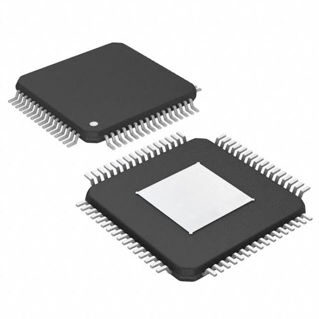
- Part No.:
- MAX9260GCB+
- Manufacturer:
- Analog Devices Inc./Maxim Integrated
- Category:
- Serializers, Deserializers
- Package:
- 64-TQFP Exposed Pad
- Datasheet:
-
 MAX9260GCB+.pdf
- Description:
- IC DESERIALIZER GMSL 64TQFP
- Quantity:
- Payment:

- Shipping:

Inventory:2,474
Please send an inquiry. Send us your inquiry, and we will respond immediately.
Product details
Overview
MAX9260GCB+ from Maxim Integrated is a gigabit multimedia deserializer for automotive serial links, supporting up to 3.125Gbps over STP cable, 1280×768 XGA display resolution, embedded I²S audio (up to 192kHz/32-bit), and full-duplex UART/I²C control channel (100kbps–1Mbps). It operates from 3.0V–3.6V AVDD/DVDD and 1.7V–3.6V IOVDD across –40°C to +105°C.
For engineers reviewing the MAX9260GCB+ datasheet, MAX9260GCB+ pinout, MAX9260GCB+ application, or MAX9260GCB+ equivalent, key selection criteria include serializer-deserializer pairing with MAX9259, spread-spectrum EMI reduction, AEC-Q100 qualification, line-fault monitoring, and automotive infotainment timing integrity under extended cable lengths.
Technical Context
The MAX9260GCB+ implements a CML-based differential receiver for high-speed serial data recovery and a parallel output interface with programmable bus width (24-/32-bit), pixel clock output (6.25–104MHz), and configurable control-channel direction (UART/I²C master/slave). Its PLL architecture supports jitter attenuation via bypass mode and deterministic lock time of ≤1500ns with spread spectrum enabled.
It integrates reverse-control-channel transceivers (IN+/IN−) with ±40mV differential thresholds, line-fault detection (LMN0/LMN1), interrupt propagation (INT), and GPIOs (GPIO0/GPIO1) - all operating within AEC-Q100 Grade 2 temperature range and compliant with ISO 10605 (±10kV contact) and IEC 61000-4-2 (±10kV contact) ESD standards.
Key Specifications
| Parameter | Value and Actual Design Meaning |
|---|---|
| Serial Data Rate | Up to 3.125Gbps - enables transmission of XGA (1280×768) video at 60Hz over 15m STP cable |
| Parallel Output Clock | PCLKOUT: 6.25–104MHz - directly drives LCD controller or FPGA video interface with <0.05UI period jitter |
| I²S Audio Support | 192kHz sample rate, 32-bit word length - delivers studio-grade audio synchronized to video with <4µs skew |
| Control Channel | Full-duplex UART/I²C link, 100kbps–1Mbps - allows host MCU on either side to configure remote peripherals without additional wiring |
| Supply Voltage | AVDD/DVDD = 3.0–3.6V; IOVDD = 1.7–3.6V - supports mixed-voltage system integration with 1.8V/3.3V logic domains |
| Operating Temperature | –40°C to +105°C - qualified per AEC-Q100 Grade 2 for under-hood and dashboard automotive placement |
| ESD Protection | ±10kV contact per ISO 10605 - ensures robustness against assembly handling and in-vehicle electrostatic discharge events |
Pinout & Package
MAX9260GCB+ is housed in a 64-pin TQFP package (10mm × 10mm × 1mm) with exposed pad (EP) connected internally to AGND and GND for thermal and electrical stability.
| Pin/Terminal | Circuit Role | Design Meaning |
|---|---|---|
| IN+, IN− | Differential Serial Input | Receives serialized video/audio/control stream from MAX9259; threshold ±40–90mV enables reliable operation over noisy automotive harnesses |
| PCLKOUT | Parallel Pixel Clock Output | Provides synchronous timing reference to display controller; programmable duty cycle (40–60%) and low jitter (<0.05UI) preserve video timing margins |
| DOUT0–DOUT28 | Parallel Video/Audio Data Outputs | Delivers unpacked RGB, sync, and auxiliary data; bus width selected by BWS pin (24-/32-bit) to match source resolution |
| ENABLE | Active-Low Output Enable | Tri-states PCLKOUT, SD, SCK, WS, and DOUT_ pins when high - enables power sequencing and hot-plug isolation |
| TX/SCL, RX/SDA | Open-Drain Control I/O | Supports bidirectional UART or I²C communication; internal 30kΩ pullups simplify interface to microcontrollers without external resistors |
| INT, LOCK, ERR | Status & Interrupt Outputs | INT signals remote-side requests; LOCK indicates stable link lock; ERR flags CRC or framing errors - enabling real-time diagnostics |
| LMN0, LMN1 | Line-Fault Monitor Inputs | Detect short-to-battery, short-to-ground, or open-circuit conditions on STP pair - critical for ASIL-B functional safety compliance |
Key Features
| Feature | Design Value |
|---|---|
| Spread-Spectrum Clocking | Programmable 0.5%/2%/4% modulation reduces peak EMI by >10dB - eliminates need for heavy shielding in camera/display cables |
| Pre/Deemphasis | Configurable transmit preemphasis and receiver equalization extend usable STP reach to 15m at full 3.125Gbps - avoids repeater ICs in mid-size vehicle architectures |
| Built-in PRBS BER Tester | On-chip pseudo-random bit sequence generator and checker enable in-system link health validation without external test equipment |
| Reverse Control Channel | Full-duplex differential UART/I²C over same STP pair - eliminates separate control wiring and reduces connector pin count by ≥30% |
| AEC-Q100 Qualified | Qualified to Grade 2 (–40°C to +105°C) with HTOL, TC, and ESD testing - meets OEM requirements for front/rear camera and infotainment modules |
Applications
| High-Resolution Automotive Navigation | Rear-Seat Infotainment |
|---|---|
Use Scenario: Central display unit receiving video from surround-view camera system via shielded twisted-pair cabling. IC Role / Device Role / Timing Role: Deserializes high-bandwidth video streams and recovers pixel clock with sub-UI jitter for seamless GUI rendering. Use Value: Enables 1280×768 navigation maps with zero frame drop over 10m harness runs, reducing latency versus LVDS solutions. | Use Scenario: Rear-seat entertainment module driving dual WVGA displays from a single media processor. IC Role / Device Role / Timing Role: Receives compressed video and audio over one serial link while routing I²S audio to local DACs. Use Value: Eliminates separate audio cables and simplifies EMI filtering - cuts BOM cost by $1.20 per seat vs. discrete audio/video interfaces. |
| Megapixel Camera Systems | ADAS Sensor Fusion Hubs |
Use Scenario: Front-facing ADAS camera transmitting 1.3MP@30fps video to domain controller through compact connector. IC Role / Device Role / Timing Role: Deserializes raw Bayer data and forwards metadata (timestamp, gain, exposure) via embedded control channel. Use Value: Supports precise timestamp alignment between camera and radar sensors using shared PCLKOUT-derived timing reference. | Use Scenario: Zonal gateway aggregating video feeds from four surround cameras into centralized perception stack. IC Role / Device Role / Timing Role: Provides synchronized parallel outputs to FPGA with deterministic delay (750–2880 bits) for multi-sensor frame alignment. Use Value: Enables hardware-level frame stitching with <1µs inter-camera skew - critical for neural network input consistency. |
Availability
MAX9260GCB+ is available at Aetrix Electronics and suitable for high-resolution automotive navigation, rear-seat infotainment, megapixel camera systems, and ADAS sensor fusion hubs requiring stable component supply across extended temperature ranges and long production lifecycles.
Supply support for MAX9260GCB+ includes scheduled delivery planning, volume procurement assistance, BOM continuity management, traceable sourcing, and lifecycle availability coordination for OEM customers, industrial embedded developers, connected-device designers, and electronics production programs.
Manufacturer
Maxim Integrated, now part of Analog Devices, designs precision analog, mixed-signal, and power management ICs for automotive, industrial, and communications applications.
The MAX9259/MAX9260 family was engineered specifically for gigabit automotive serial links - delivering high-speed video, embedded audio, and bidirectional control over a single STP pair while meeting stringent AEC-Q100 and ESD requirements.
FAQ
What is the primary function of the MAX9260GCB+ in a serial link system?
The MAX9260GCB+ is a deserializer that receives high-speed serialized video, audio, and control data over a differential STP link from the MAX9259 serializer. It reconstructs parallel video outputs (DOUT0–DOUT28), generates PCLKOUT, recovers I²S audio signals (SD/SCK/WS), and manages bidirectional UART/I²C communication - all while maintaining AEC-Q100 compliance and EMI robustness.
Does the MAX9260GCB+ require an external crystal or oscillator?
No, the MAX9260GCB+ does not require an external crystal or oscillator. It recovers the serial clock embedded in the incoming CML data stream from the MAX9259 and uses this recovered clock to generate its PCLKOUT and internal timing - eliminating BOM cost and board space associated with discrete timing components.
Can the MAX9260GCB+ operate with different bus widths, and how is this configured?
Yes, the MAX9260GCB+ supports both 24-bit and 32-bit parallel output modes. Bus width is selected via the BWS pin: BWS = low configures 24-bit mode (RGB + sync), while BWS = high enables 32-bit mode (RGB + sync + two auxiliary data bits). This configuration is latched at power-up or wake-from-power-down.
How does the MAX9260GCB+ handle electromagnetic interference (EMI) in automotive environments?
The MAX9260GCB+ reduces EMI through programmable spread-spectrum clocking (0.5%, 2%, or 4% modulation), differential CML signaling with controlled output voltage (300–500mVP-P), and integrated pre/deemphasis. These features lower peak radiated emissions by >10dB, allowing compliance with CISPR 25 Class 5 without added ferrites or shielding.
Is the MAX9260GCB+ pin-compatible with other devices in the MAX9259/MAX9260 family?
The MAX9260GCB+ shares the same 64-pin TQFP package and core pinout with other MAX9260 variants (e.g., MAX9260GTN/V+T), but is not pin-compatible with MAX9259 serializers or QFND-packaged MAX9260 versions. Signal mapping and power domains (3.3V AVDD vs. 1.8V for MAX9259) differ fundamentally between serializer and deserializer roles.
MAX9260GCB+ Specifications
- Product attributes
- Attribute value
- Manufacturer:
- Analog Devices Inc./Maxim Integrated
- Series:
- -
- Package/Case:
- 64-TQFP Exposed Pad
- Packaging:
- Tray
- Product Status:
- Active
- Function:
- Deserializer
- Data Rate:
- 2.5Gbps
- Input Type:
- CML
- Output Type:
- CMOS, LVCMOS
- Number of Inputs:
- 1
- Number of Outputs:
- 30
- Voltage - Supply:
- 1.7V ~ 3.6V
- Operating Temperature:
- -40°C ~ 105°C (TA)
- Grade:
- -
- Qualification:
- -
- Mounting Type:
- Surface Mount
- Supplier Device Package:
- 64-TQFP-EP (10x10)
MAX9260GCB+ FAQ
1.How can I place an order for MAX9260GCB+ through Aetrix?
Please submit a Request for Quotation (RFQ) for MAX9260GCB+ on Aetrix. Our sales agent will provide a competitive quotation and guide you through the order confirmation once you accept the terms.
2.Are the price and stock information for MAX9260GCB+ reliable?
The price and inventory of MAX9260GCB+ are updated periodically and may fluctuate due to market conditions. Stock and pricing data are typically refreshed every 24 hours. Quotation validity for MAX9260GCB+ is usually 5 days.
3.What payment methods are accepted for MAX9260GCB+?
We accept Wire Transfer, PayPal, Credit Card, Western Union, MoneyGram, and Escrow for MAX9260GCB+ transactions.
Note: Certain payment methods may incur a processing fee.
4.How is shipping managed for MAX9260GCB+?
MAX9260GCB+ orders can be shipped via leading logistics carriers, including DHL, UPS, FedEx, TNT, or Registered Mail.
Once your MAX9260GCB+ order is processed, you will receive an email with the shipment details and tracking number.
Note: Tracking information may take up to 24 hours to appear. Express delivery typically takes 3–5 business days.
5.How can I obtain technical support or documentation for MAX9260GCB+?
For technical support, including MAX9260GCB+ datasheets, pinout diagrams, or application guidance, please contact our engineering support team. They can provide detailed documentation and assistance for your MAX9260GCB+ requirements.
6.How does Aetrix verify that MAX9260GCB+ is sourced from the original manufacturer or authorized distributors?
All MAX9260GCB+ products on Aetrix are procured from qualified distributors and authorized channels. Our dedicated quality assurance team conducts strict verification, including traceability checks and, if necessary, third-party testing. This ensures that MAX9260GCB+ meets industry standards.
7.What is the process for return or replacement of MAX9260GCB+?
All MAX9260GCB+ units undergo pre-shipment inspection (PSI). If there is an issue with MAX9260GCB+, returns or replacements are accepted under the following conditions:
1.Quantity discrepancies, incorrect items, or visible external defects (such as breakage or corrosion), acknowledged by Aetrix.
2.The issue is reported within 90 days of delivery.
3.The MAX9260GCB+ part is unused and in its original packaging.
Return procedure for MAX9260GCB+:
1.Submit a request within 90 days.
2.Obtain a Return Material Authorization (RMA) from Aetrix.
MAX9260GCB+ Tags

-
SN65HVS880PWPR
Texas Instruments
-
SN65HVS882PWPR
Texas Instruments

-
FIN3386MTDX
onsemi
-
FIN3385MTDX
onsemi

-
SN65LV1023ARHBR
Texas Instruments

-
SN65LV1023ADBR
Texas Instruments
-
SN65LV1224BDBR
Texas Instruments

-
SN65LVDS93ADGGR
Texas Instruments
-
SN65LVDS93DGGR
Texas Instruments

-
TDES954RGZT
Texas Instruments
-
SN65LV1224BRHBT
Texas Instruments

-
DS90UB914QSQE/NOPB
Texas Instruments
Tech Hub

A practical engineering guide to 3.3V and 5V logic compatibility, input thresholds, resistor dividers, translator ICs, MOSFET level shifting, I2C pull-ups, timing limits and power-sequencing risks.

The 74HC595 uses push-pull logic outputs, while the TPIC6B595 uses 50 V open-drain DMOS sinks for higher-power loads. This guide compares timing, current limits, 3.3 V interfacing, load wiring, thermal…

The 74HC595 converts serial data into eight stable parallel outputs. This guide covers pin functions, shift and storage timing, OE and MR behavior, drive-current limits, cascading, voltage compatibilit…

A technical comparison of level-sensitive latches and edge-triggered flip-flops, covering timing windows, setup and hold limits, master–slave operation, time borrowing, race-through, HDL inference and…

A D latch stores one bit while Enable controls when data can pass. This reference covers gate-level operation, truth tables, transparency, setup and hold timing, LE versus OE, common ICs and practical …

An SR latch stores one bit through cross-coupled feedback. This engineering reference covers NOR and NAND implementations, truth tables, forbidden-state recovery, gated operation, switch debouncing, fa…

Latch circuits retain one bit through feedback. This technical reference covers SR and D latches, truth tables, transparency, timing limits, latch-versus-flip-flop behavior, applications and common log…

An engineering guide to LED driver operation, constant-current and constant-voltage outputs, linear and switching topologies, dimming, IC selection, calculations, replacement compatibility, and fault c…

Operational amplifier guide covering op amp basics, feedback, ideal vs real op amps, common configurations, buffer circuits, offset, bias current, gain-bandwidth, slew rate, rail-to-rail limits and sel…

Jumper cables guide covering safe connection order, red and black clamp placement, final ground connection, cable gauge, length, clamp quality, copper vs CCA cables, jump starter comparison and battery…


