
 My Inquiry
 My Account


Analog Devices Inc./Maxim Integrated MAX9270GTN/V+
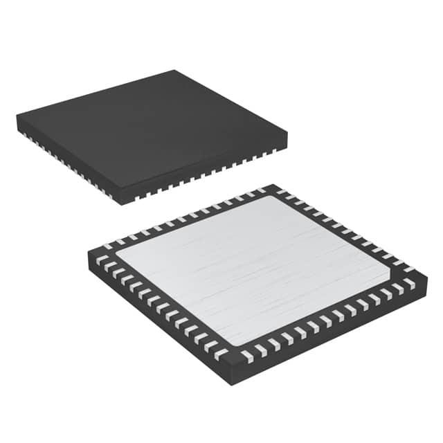
- Part No.:
- MAX9270GTN/V+
- Manufacturer:
- Analog Devices Inc./Maxim Integrated
- Category:
- Serializers, Deserializers
- Package:
- 56-WFQFN Exposed Pad
- Datasheet:
-
 MAX9270GTN/V+.pdf
- Description:
- IC SUPERVISOR
- Quantity:
- Payment:

- Shipping:

Inventory:5,164
Please send an inquiry. Send us your inquiry, and we will respond immediately.
Product details
Overview
MAX9270GTN/V+ from Maxim Integrated is a gigabit multimedia deserializer implementing GMSL technology for automotive video and image-sensing links. It accepts up to 2.5Gbps serial payload over 15m STP cable, delivers 24-bit or 32-bit parallel output at up to 104MHz or 78MHz respectively, and integrates a full-duplex 100kbps–1Mbps UART control channel. It enables XGA display panels (1280×768) or dual-view WVGA (2×854×480) in infotainment systems.
For engineers reviewing the MAX9270GTN/V+ datasheet, MAX9270GTN/V+ pinout, MAX9270GTN/V+ application, or MAX9270GTN/V+ equivalent, this page provides verified technical context, validated pin functions, confirmed automotive-grade operating range (−40°C to +105°C), spread-spectrum EMI reduction capability, and real-world control-channel configuration options for display and camera subsystems.
Technical Context
The MAX9270GTN/V+ implements a CDR-based 8b/10b-decoding architecture with integrated line equalizer (5.2dB or 10.7dB boost selectable via EQS pin) and dual PLLs for clock recovery and parallel clock generation. Its reverse control channel uses differential CML signaling on IN+/IN− for bidirectional UART communication between serializer and deserializer.
It supports auto data-rate detection and programmable spread spectrum on parallel outputs (enabled via SSEN pin), while eliminating the ENABLE pin found on MAX9260-output enable is instead controlled by register bit OUTENB. The device operates with 3.3V core (AVDD/DVDD) and 1.8V–3.3V I/O (IOVDD) supplies, meeting ISO 10605 and IEC 61000-4-2 ESD requirements.
Key Specifications
| Parameter | Value and Actual Design Meaning |
|---|---|
| Serial Data Rate | Up to 2.5Gbps payload over AC-coupled STP; supports 15m cable length at BER < 10⁻⁹. |
| Parallel Bus Width | Programmable 24-bit (DOUT0–DOUT20 + SYNC) or 32-bit (DOUT0–DOUT28); BWS pin selects mode. |
| Parallel Clock Frequency | 8.33–104MHz (24-bit) or 6.25–78MHz (32-bit); DRS pin selects high/low range. |
| Control Channel | Full-duplex differential UART (100kbps–1Mbps); supports I²C base mode or user-defined bypass mode. |
| Operating Temperature | −40°C to +105°C; qualified per AEC-Q100 for automotive navigation, infotainment, and ADAS camera systems. |
| Supply Voltages | 3.3V core (AVDD/DVDD); 1.8V–3.3V I/O (IOVDD); exposed pad (EP) must be connected to PCB ground. |
| ESD Protection | ±8kV contact / ±10kV air (IEC 61000-4-2); ±8kV contact / ±20kV air (ISO 10605) on IN+/IN− pins. |
Pinout & Package
The MAX9270GTN/V+ is housed in a 56-pin TQFN package (8mm × 8mm × 0.75mm) with exposed pad (EP), requiring connection to PCB ground for thermal and electrical performance.
| Pin/Terminal | Circuit Role | Design Meaning |
|---|---|---|
| BWS (Pin 1) | Bus-width select input | Configures parallel bus as 24-bit (low) or 32-bit (high); requires external pullup/pulldown. |
| INT (Pin 2) | Interrupt input | Toggles serializer INT output on transition; supports touch-screen interrupt forwarding. |
| CDS (Pin 3) | Control-direction selection | Determines host ECU location: low = ECU on serializer side; high = ECU on deserializer side. |
| GPIO0/GPIO1 (Pins 4,10) | Open-drain GPIO | Internal 60kΩ pullup to IOVDD; high-impedance during power-up and PWDN assertion. |
| IN+/IN− (Pins 7,8) | Differential CML serial input | Accepts GMSL-encoded 2.5Gbps stream; compliant with ISO 10605 and IEC 61000-4-2 ESD standards. |
| PCLKOUT (Pin 36) | Parallel clock output | Strobes DOUT0–DOUT28; edge selectable (ES pin); frequency set by DRS/BWS configuration. |
| RX/SDA & TX/SCL (Pins 14,15) | I²C/UART bidirectional interface | Shared pins for control channel: RX/SDA = I²C data or UART Rx; TX/SCL = I²C clock or UART Tx. |
| SSEN (Pin 54) | Spread-spectrum enable | Enables/disables 2% spread spectrum on parallel outputs to reduce EMI; latched at power-up. |
Key Features
| Feature | Design Value |
|---|---|
| GMSL serializer pairing | Interoperates with any Maxim GMSL serializer (e.g., MAX9269, MAX9271), enabling flexible system-level link design without vendor lock-in. |
| Auto data-rate detection | Eliminates manual configuration: detects incoming serial data rate "on-the-fly" and adapts PLL and FIFO timing accordingly. |
| Embedded PRBS checker | On-chip bit-error-rate testing capability; enables in-system link integrity validation without external test equipment. |
| Programmable equalizer | Two fixed gain settings (5.2dB or 10.7dB) selected by EQS pin; extends reliable link length over aging or marginal STP cables. |
| Separate LOCK and ERR signals | LOCK indicates PLL lock and word-boundary alignment; ERR flags decoding errors or PRBS failures-enabling robust diagnostics in safety-critical systems. |
| No external clock required | Self-contained clock recovery eliminates need for reference clock distribution, reducing board complexity and jitter sources. |
Applications
| Automotive Infotainment Display | ADAS Camera Interface |
|---|---|
Use Scenario: High-resolution video transmission from central ECU to TFT-LCD dashboard display in vehicle cockpit. IC Role / Device Role / Timing Role: Deserializes GMSL-encoded video/audio/control stream; generates synchronized PCLKOUT and parallel RGB+SYNC outputs for display controller interface. Use Value: Supports XGA (1280×768) resolution at 104MHz with embedded I²C control of backlight and gamma correction-reducing wiring harness weight and EMI vs. parallel LVCMOS. |
Use Scenario: Front-facing camera module sending raw image data to domain controller for lane-departure or AEB processing. IC Role / Device Role / Timing Role: Receives serialized sensor data; outputs 24-bit pixel data at 78MHz with precise timing alignment to support three 10-bit camera links simultaneously. Use Value: Enables dual-view WVGA (2×854×480) or single high-res stream with built-in error detection (ERR signal) and lock status (LOCK) for functional safety monitoring. |
| Touch-Screen Integration | In-Cabin Occupancy Sensing |
Use Scenario: Coordinating capacitive touch controller response with displayed UI elements in center-stack touchscreen. IC Role / Device Role / Timing Role: Routes touch interrupts via INT pin to serializer; forwards I²C commands from host ECU to touch IC using embedded control channel. Use Value: Eliminates separate I²C bus routing-touch events are synchronized to video frame boundaries via shared GMSL link, reducing latency and connector count. |
Use Scenario: Transmitting IR or time-of-flight sensor data from rear-seat occupancy module to body control unit. IC Role / Device Role / Timing Role: Deserializes low-bandwidth sensor metadata and control signals; uses GPIO0/GPIO1 for local presence detection status reporting. Use Value: Leverages same STP cable used for primary video link-no additional cabling needed; supports remote I²C peripheral access (e.g., ambient light sensor) via bypass-mode UART. |
Equivalent & Alternatives
The following parts are listed as comparable options for similar gigabit multimedia deserializer applications.
| Alternative Part | Technical Difference | Application Difference | Selection Advice |
|---|---|---|---|
| MAX9272GTN/V+ | Includes dedicated ENABLE pin; otherwise identical GMSL functionality, pinout, and specs. | Required where hardware-level output gating is needed (e.g., dynamic panel power sequencing). | Select MAX9272GTN/V+ only if explicit hardware output enable is mandated; MAX9270GTN/V+ uses register-controlled enable (OUTENB) and saves one PCB trace. |
| MAX9296A GTN/V+ | Higher serial rate (3.125Gbps); supports 4-lane MIPI-CSI2 output; larger 64-pin TQFN package. | Targets higher-resolution cameras (e.g., 4MP+ sensors) and multi-camera fusion systems requiring MIPI compatibility. | Choose MAX9296A GTN/V+ for next-gen ADAS with >2MP imaging; MAX9270GTN/V+ remains optimal for cost-sensitive XGA/WVGA display and entry-level camera links. |
Compared with MAX9272GTN/V+, the MAX9270GTN/V+ removes the ENABLE pin in favor of register-based output control-reducing PCB routing overhead without sacrificing functionality. Against MAX9296A GTN/V+, it offers lower cost and smaller footprint for applications within 2.5Gbps and parallel RGB interface requirements.
Availability
MAX9270GTN/V+ is available at Aetrix Electronics and suitable for automotive infotainment displays, ADAS camera interfaces, and in-cabin sensing systems requiring stable component supply across extended temperature ranges and long production lifecycles.
Supply support for MAX9270GTN/V+ includes scheduled delivery planning, volume procurement assistance, BOM continuity management, traceable sourcing, and lifecycle availability coordination for OEM customers, industrial embedded developers, connected-device designers, and electronics production programs.
Manufacturer
Maxim Integrated (now part of Analog Devices) designs precision analog, mixed-signal, and power management ICs for automotive, industrial, and communications markets.
The MAX9270GTN/V+ belongs to Maxim's GMSL serializer/deserializer product line, engineered specifically for high-reliability, low-EMI, long-cable automotive video and sensor data transmission with integrated control-channel intelligence.
FAQ
What is the maximum supported cable length for MAX9270GTN/V+ at full 2.5Gbps data rate?
The MAX9270GTN/V+ supports up to 15 meters of shielded twisted-pair (STP) cable at 2.5Gbps payload rate with BER < 10⁻⁹, as validated in the datasheet's typical operating characteristics. Link reliability beyond 15m depends on cable quality and equalizer setting (EQS pin); use EQS = low for 10.7dB boost to extend reach in marginal installations. The MAX9270GTN/V+ does not require repeaters within this range.
Does MAX9270GTN/V+ support both I²C and UART protocols on its control channel?
Yes, the MAX9270GTN/V+ supports both protocols via the same RX/SDA and TX/SCL pins. Base mode uses standard I²C (configured by MS = low and CDS = high), while bypass mode enables full-duplex user-defined UART (MS = high). The protocol selection is determined by pin strapping at power-up and cannot be changed dynamically in operation without reset.
How is output enable implemented on MAX9270GTN/V+ since it lacks an ENABLE pin?
The MAX9270GTN/V+ replaces the hardware ENABLE pin (present on MAX9260) with register-controlled output enable. Bit OUTENB in register 0x04 determines whether parallel outputs (DOUT0–DOUT28) and PCLKOUT are active. This allows firmware-level control without additional PCB routing-unlike the MAX9270GTN/V+, which relies solely on pin-strapped configuration.
Can MAX9270GTN/V+ drive a 1280×768 XGA display directly?
Yes, the MAX9270GTN/V+ supports XGA resolution in 24-bit mode at up to 104MHz PCLKOUT, delivering RGB (24 bits), HSYNC, VSYNC, and DE signals across DOUT0–DOUT20. It requires no external logic translation and maintains timing alignment per JEDEC standards. The MAX9270GTN/V+ also embeds I²C master capability to configure display timing controllers or backlight ICs over the same GMSL link.
What is the function of the LOCK and ERR pins on MAX9270GTN/V+?
LOCK is an open-drain output indicating PLL lock and correct serial-word-boundary alignment-driven high when locked, low otherwise. ERR is also open-drain and asserts low when decoding errors exceed threshold or PRBS test fails. Both signals remain high-impedance during power-down (PWDN = low). These pins provide real-time hardware diagnostics critical for automotive ASIL-B compliance in MAX9270GTN/V+ systems.
MAX9270GTN/V+ Specifications
- Product attributes
- Attribute value
- Manufacturer:
- Analog Devices Inc./Maxim Integrated
- Series:
- -
- Package/Case:
- 56-WFQFN Exposed Pad
- Packaging:
- Tube
- Product Status:
- Obsolete
- Function:
- Deserializer
- Data Rate:
- 104MHz
- Input Type:
- CML
- Output Type:
- Parallel
- Number of Inputs:
- 1
- Number of Outputs:
- 29
- Voltage - Supply:
- 1.8V ~ 3.3V
- Operating Temperature:
- -40°C ~ 105°C
- Grade:
- Automotive
- Qualification:
- AEC-Q100
- Mounting Type:
- Surface Mount
- Supplier Device Package:
- 56-TQFN (8x8)
MAX9270GTN/V+ FAQ
1.How can I place an order for MAX9270GTN/V+ through Aetrix?
Please submit a Request for Quotation (RFQ) for MAX9270GTN/V+ on Aetrix. Our sales agent will provide a competitive quotation and guide you through the order confirmation once you accept the terms.
2.Are the price and stock information for MAX9270GTN/V+ reliable?
The price and inventory of MAX9270GTN/V+ are updated periodically and may fluctuate due to market conditions. Stock and pricing data are typically refreshed every 24 hours. Quotation validity for MAX9270GTN/V+ is usually 5 days.
3.What payment methods are accepted for MAX9270GTN/V+?
We accept Wire Transfer, PayPal, Credit Card, Western Union, MoneyGram, and Escrow for MAX9270GTN/V+ transactions.
Note: Certain payment methods may incur a processing fee.
4.How is shipping managed for MAX9270GTN/V+?
MAX9270GTN/V+ orders can be shipped via leading logistics carriers, including DHL, UPS, FedEx, TNT, or Registered Mail.
Once your MAX9270GTN/V+ order is processed, you will receive an email with the shipment details and tracking number.
Note: Tracking information may take up to 24 hours to appear. Express delivery typically takes 3–5 business days.
5.How can I obtain technical support or documentation for MAX9270GTN/V+?
For technical support, including MAX9270GTN/V+ datasheets, pinout diagrams, or application guidance, please contact our engineering support team. They can provide detailed documentation and assistance for your MAX9270GTN/V+ requirements.
6.How does Aetrix verify that MAX9270GTN/V+ is sourced from the original manufacturer or authorized distributors?
All MAX9270GTN/V+ products on Aetrix are procured from qualified distributors and authorized channels. Our dedicated quality assurance team conducts strict verification, including traceability checks and, if necessary, third-party testing. This ensures that MAX9270GTN/V+ meets industry standards.
7.What is the process for return or replacement of MAX9270GTN/V+?
All MAX9270GTN/V+ units undergo pre-shipment inspection (PSI). If there is an issue with MAX9270GTN/V+, returns or replacements are accepted under the following conditions:
1.Quantity discrepancies, incorrect items, or visible external defects (such as breakage or corrosion), acknowledged by Aetrix.
2.The issue is reported within 90 days of delivery.
3.The MAX9270GTN/V+ part is unused and in its original packaging.
Return procedure for MAX9270GTN/V+:
1.Submit a request within 90 days.
2.Obtain a Return Material Authorization (RMA) from Aetrix.
MAX9270GTN/V+ Tags

-
SN65HVS880PWPR
Texas Instruments
-
SN65HVS882PWPR
Texas Instruments

-
FIN3386MTDX
onsemi
-
FIN3385MTDX
onsemi

-
SN65LV1023ARHBR
Texas Instruments

-
SN65LV1023ADBR
Texas Instruments
-
SN65LV1224BDBR
Texas Instruments

-
SN65LVDS93ADGGR
Texas Instruments
-
SN65LVDS93DGGR
Texas Instruments

-
TDES954RGZT
Texas Instruments
-
SN65LV1224BRHBT
Texas Instruments

-
DS90UB914QSQE/NOPB
Texas Instruments
Tech Hub

A practical engineering guide to 3.3V and 5V logic compatibility, input thresholds, resistor dividers, translator ICs, MOSFET level shifting, I2C pull-ups, timing limits and power-sequencing risks.

The 74HC595 uses push-pull logic outputs, while the TPIC6B595 uses 50 V open-drain DMOS sinks for higher-power loads. This guide compares timing, current limits, 3.3 V interfacing, load wiring, thermal…

The 74HC595 converts serial data into eight stable parallel outputs. This guide covers pin functions, shift and storage timing, OE and MR behavior, drive-current limits, cascading, voltage compatibilit…

A technical comparison of level-sensitive latches and edge-triggered flip-flops, covering timing windows, setup and hold limits, master–slave operation, time borrowing, race-through, HDL inference and…

A D latch stores one bit while Enable controls when data can pass. This reference covers gate-level operation, truth tables, transparency, setup and hold timing, LE versus OE, common ICs and practical …

An SR latch stores one bit through cross-coupled feedback. This engineering reference covers NOR and NAND implementations, truth tables, forbidden-state recovery, gated operation, switch debouncing, fa…

Latch circuits retain one bit through feedback. This technical reference covers SR and D latches, truth tables, transparency, timing limits, latch-versus-flip-flop behavior, applications and common log…

An engineering guide to LED driver operation, constant-current and constant-voltage outputs, linear and switching topologies, dimming, IC selection, calculations, replacement compatibility, and fault c…

Operational amplifier guide covering op amp basics, feedback, ideal vs real op amps, common configurations, buffer circuits, offset, bias current, gain-bandwidth, slew rate, rail-to-rail limits and sel…

Jumper cables guide covering safe connection order, red and black clamp placement, final ground connection, cable gauge, length, clamp quality, copper vs CCA cables, jump starter comparison and battery…


