
 My Inquiry
 My Account


Analog Devices Inc./Maxim Integrated MAX934CPE
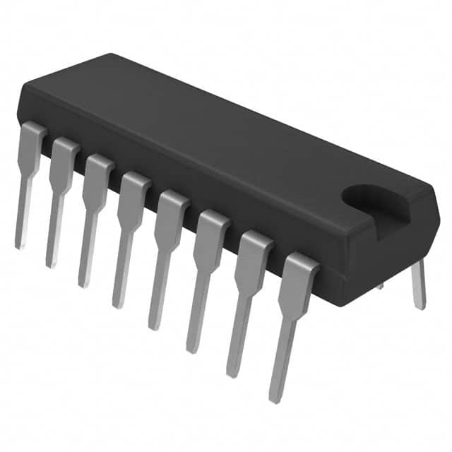
- Part No.:
- MAX934CPE
- Manufacturer:
- Analog Devices Inc./Maxim Integrated
- Category:
- Comparators
- Package:
- 16-DIP (0.300", 7.62mm)
- Datasheet:
-
 MAX934CPE.pdf
- Description:
- IC COMPARATOR 4 W/VOLT REF 16DIP
- Quantity:
- Payment:

- Shipping:

Inventory:3,013
Please send an inquiry. Send us your inquiry, and we will respond immediately.
Product details
Overview
MAX934CPE from Maxim Integrated is a quad micropower comparator with integrated 1.182V ±2% bandgap reference, designed for ultra-low-power single-supply systems. It delivers <4µA quiescent current (typ. 3.5µA at 5V), supports 2.5V–11V operation, features rail-to-rail input range (V− to V+ −1.3V), and provides TTL/CMOS-compatible outputs sourcing up to 40mA - ideal for battery-powered threshold detection and window monitoring.
For engineers reviewing the MAX934CPE datasheet, MAX934CPE pinout, MAX934CPE application, or MAX934CPE equivalent, key selection considerations include its quad-comparator architecture with independent inputs/outputs, internal reference referenced to V− (not GND), hysteresis implementation via external feedback (not HYST pin), and compatibility with 0°C to +70°C commercial temperature range in 16-pin plastic DIP package.
Technical Context
The MAX934CPE integrates four independent comparators and a precision 1.182V reference referenced to V−, enabling self-contained voltage monitoring without external references. Its output stage sources up to 40mA continuously and sinks >5mA while maintaining sub-4µA supply current - achieved via crowbar-free switching that eliminates supply glitches during transitions.
Unlike MAX931–MAX933, the MAX934CPE lacks a dedicated HYST pin; hysteresis must be implemented externally using positive feedback resistors per comparator. Input common-mode range extends from V− to V+ −1.3V, supporting operation down to 2.5V total supply (±1.25V dual), with guaranteed functionality to 1V only in low-voltage test conditions (not specified for production use).
Key Specifications
| Parameter | Value and Actual Design Meaning |
|---|---|
| Supply Voltage Range | Single +2.5V to +11V or dual ±1.25V to ±5.5V - enables direct interface with 3V/5V logic and bipolar sensor signals. |
| Quiescent Supply Current | <4µA max over temperature - ensures multi-year battery life in always-on monitoring applications. |
| Reference Voltage | 1.182V ±2% (0°C to +70°C), referenced to V− - provides stable trip point without external components; not bypassed. |
| Input Common-Mode Range | V− to V+ −1.3V - allows direct sensing of signals near ground or rail in single-supply configurations. |
| Output Drive Capability | Sources 40mA continuously, sinks 5mA minimum - drives LEDs, MOSFET gates, or logic inputs directly without buffers. |
| Propagation Delay | 12µs typical (10mV overdrive) - balances speed and power for low-frequency threshold detection. |
| Reference Load Capacity | Sinks 8µA / sources 15µA - supports biasing of up to two comparator HYST inputs or small resistor dividers. |
Pinout & Package
MAX934CPE is housed in a 16-pin plastic DIP package (0°C to +70°C commercial grade), with through-hole mounting and 0.3-inch width. Pin spacing follows JEDEC MS-001 standard.
| Pin/Terminal | Circuit Role | Design Meaning |
|---|---|---|
| 1 | OUTB | Comparator B output: TTL/CMOS-compatible, swings V+ to GND; sources 40mA, sinks 5mA. |
| 2 | OUTA | Comparator A output: identical drive capability and swing range as OUTB. |
| 3 | V+ | Positive supply input: accepts 2.5V–11V single or +5.5V in dual-supply mode. |
| 4 | INA− | Inverting input of comparator A: supports common-mode range from V− to V+ −1.3V. |
| 5 | INA+ | Noninverting input of comparator A: matched offset and leakage (<±10mV, <±0.01nA). |
| 6 | INB− | Inverting input of comparator B: electrically identical to INA−; no shared internal nodes. |
| 7 | INB+ | Noninverting input of comparator B: independent of other comparator inputs. |
| 8 | REF | Reference output: 1.182V ±2% w.r.t. V−; not referenced to GND; avoid capacitive coupling. |
| 9 | V− | Negative supply: connect to GND for single-supply operation; defines REF and input common-mode baseline. |
| 10 | INC− | Inverting input of comparator C: fully isolated; supports same voltage range as INA−. |
| 11 | INC+ | Noninverting input of comparator C: matched performance to INA+/INB+. |
| 12 | IND− | Inverting input of comparator D: independent channel with rail-to-rail input capability. |
| 13 | IND+ | Noninverting input of comparator D: enables four-channel differential sensing. |
| 14 | GND | Ground connection: tied internally to V− for single-supply use; separates output driver return path. |
| 15 | OUTD | Comparator D output: identical electrical specs to OUTA/OUTB/OUTC. |
| 16 | OUTC | Comparator C output: full drive strength and logic compatibility; no shared output stage. |
Key Features
| Feature | Design Value |
|---|---|
| Quad comparator + reference integration | Reduces BOM count by eliminating four discrete comparators and one precision reference IC. |
| Crowbar-free output stage | Prevents supply-line transients during switching, eliminating need for heavy local bypassing. |
| Rail-to-rail input range (V− to V+ −1.3V) | Enables direct sensing of 0V-referenced signals (e.g., battery voltage, sensor outputs) without level-shifting. |
| 40mA continuous output source current | Drives LEDs, small relays, or MOSFET gates directly - avoids external driver stages in portable designs. |
| 1.182V ±2% internal reference | Provides stable trip voltage across temperature; referenced to V−, simplifying single-supply bias networks. |
| No HYST pin (external hysteresis only) | Allows per-comparator hysteresis tuning via feedback resistors - critical for asymmetric window thresholds. |
Applications
| Battery-Powered Threshold Detector | Quad Window Comparator |
|---|---|
|
Use Scenario: Monitoring lithium-ion cell voltage (2.5V–4.2V) to trigger low-battery warning and overvoltage cutoff in handheld medical devices. IC Role / Device Role / Timing Role: MAX934CPE acts as four independent voltage comparators: two for undervoltage/overvoltage thresholds, two for hysteresis control and status latching. Use Value: Sub-4µA quiescent current extends battery life beyond 5 years in sleep mode; integrated reference eliminates calibration drift vs. resistor-divider solutions. |
Use Scenario: Validating 5V power rail integrity in industrial PLC I/O modules with separate under/overvoltage alarms. IC Role / Device Role / Timing Role: MAX934CPE implements dual-window detection: comparators A/B monitor upper/lower bounds, C/D generate latched fault flags with programmable hysteresis. Use Value: Four-channel integration reduces PCB area by 60% vs. discrete solutions; rail-to-rail inputs accept direct 5V rail sampling without attenuation. |
| LED Bar-Graph Level Gauge | Multi-Stage Low-Voltage Detector |
|
Use Scenario: Visualizing analog sensor output (e.g., pressure, temperature) as 4-segment LED display in HVAC control panels. IC Role / Device Role / Timing Role: MAX934CPE's four comparators drive individual LEDs via current-limiting resistors; REF sets uniform trip points across all segments. Use Value: 40mA output drive powers LEDs directly - no transistor buffers needed; integrated reference ensures consistent brightness and threshold accuracy. |
Use Scenario: Sequencing power-down in automotive infotainment systems when 12V battery drops below 11.5V, then 10.5V, then 9.0V. IC Role / Device Role / Timing Role: MAX934CPE configures three comparators as cascaded thresholds (LOW/FAIL/CRITICAL), fourth as logic OR for system reset assertion. Use Value: Single-package solution replaces three discrete comparators and reference; V− referenced design simplifies grounding in noisy vehicle electrical environments. |
Equivalent & Alternatives
The following parts are listed as comparable options for similar quad comparator with reference applications.
| Alternative Part | Technical Difference | Application Difference | Selection Advice |
|---|---|---|---|
| MAX934EPE | Same die, extended −40°C to +85°C temperature range; higher max supply current (4.5µA vs. 3.5µA typ. at 5V). | Required for automotive or outdoor industrial deployments; not suitable for cost-sensitive commercial-grade products. | Select MAX934EPE when operating ambient exceeds +70°C; otherwise MAX934CPE offers lower cost and verified stability at room temperature. |
| MAX924CPE | Pin-compatible quad comparator with 1% reference accuracy (1.182V ±1%), higher quiescent current (5µA max), same package and pinout. | Used where tighter trip-point tolerance is mandatory (e.g., precision power sequencing), accepting 25% higher supply current. | Choose MAX924CPE only if ±1% reference accuracy is required; MAX934CPE provides optimal power/accuracy trade-off for general-purpose monitoring. |
Compared with MAX934EPE, the MAX934CPE trades extended temperature capability for lower cost and marginally better quiescent current; compared with MAX924CPE, it sacrifices 1% reference accuracy to achieve 20% lower supply current - making it optimal for battery-critical, cost-sensitive commercial applications.
Availability
MAX934CPE is available at Aetrix Electronics and suitable for battery-powered systems, threshold detectors, window comparators, and oscillator circuits requiring stable component supply with commercial-temperature assurance.
Supply support for MAX934CPE includes scheduled delivery planning, volume procurement assistance, BOM continuity management, traceable sourcing, and lifecycle availability coordination for OEM customers, industrial embedded developers, connected-device designers, and electronics production programs.
Manufacturer
Maxim Integrated (now part of Analog Devices) designs precision analog and mixed-signal ICs for power, sensing, and interface applications, with emphasis on low-power innovation.
The MAX931–MAX934 family was engineered specifically for micropower voltage monitoring in portable and energy-constrained systems, integrating reference and comparator functions to minimize external components and standby current.
FAQ
What is the maximum supply voltage for MAX934CPE in single-supply operation?
The MAX934CPE supports single-supply operation from +2.5V to +11V. At +11V, the device remains within Absolute Maximum Ratings (V+ to V− ≤ +12V), and all electrical specifications - including reference accuracy, propagation delay, and output drive - are guaranteed across the 0°C to +70°C commercial temperature range. Operation above +11V risks permanent damage.
Does MAX934CPE have an internal HYST pin like MAX931–MAX933?
No, the MAX934CPE does not include a HYST pin. Hysteresis must be implemented externally using positive feedback resistors on each comparator's inputs, as shown in Figure 4 of the datasheet. This differs from MAX931/MAX932/MAX933, which feature a dedicated HYST terminal for simplified hysteresis programming with two resistors.
Can the reference output (REF) of MAX934CPE be used to bias external circuitry?
Yes, the REF pin of MAX934CPE can source up to 15µA or sink up to 8µA while maintaining ±2% accuracy. It is commonly used to set trip thresholds for all four comparators via resistor dividers. However, do not bypass REF with capacitors - doing so causes instability due to crosstalk-induced noise amplification.
What is the input offset voltage specification for MAX934CPE?
The MAX934CPE has a maximum input offset voltage of ±10mV over the full commercial temperature range (0°C to +70°C). This value is measured differentially between IN+ and IN− pins of any comparator, with V+ = 5V and V− = GND. Offset remains stable across supply voltages from 2.5V to 11V, enabling accurate threshold setting in varying battery conditions.
Is MAX934CPE pin-compatible with any higher-accuracy alternatives?
Yes, MAX934CPE is pin-compatible with MAX924CPE, which offers 1% reference accuracy (vs. 2%) and identical 16-pin DIP packaging. Both share identical pin assignments, thermal characteristics, and footprint - allowing drop-in replacement where tighter reference tolerance is required, though MAX924CPE draws ~25% more quiescent current.
MAX934CPE Specifications
- Product attributes
- Attribute value
- Manufacturer:
- Analog Devices Inc./Maxim Integrated
- Package/Case:
- 16-DIP (0.300", 7.62mm)
- Series:
- -
- Packaging:
- Tube
- Product Status:
- Obsolete
- Type:
- with Voltage Reference
- Number of Elements:
- 4
- Output Type:
- CMOS, TTL
- Voltage - Supply, Single/Dual (±):
- 2.5V ~ 11V, ±1.25V ~ 5.5V
- :
- 10mV @ 5V
- Voltage - Input Offset (Max):
- -
- Current - Input Bias (Max):
- 0.015mA @ 5V
- Current - Output (Typ):
- 8.5µA
- Current - Quiescent (Max):
- 80dB CMRR, 80dB PSRR
- CMRR, PSRR (Typ):
- 12µs
- Propagation Delay (Max):
- -
- Hysteresis:
- 0°C ~ 70°C
- Operating Temperature:
- -
- Grade:
- -
- Qualification:
- Through Hole
- :
- 16-PDIP
MAX934CPE FAQ
1.How can I place an order for MAX934CPE through Aetrix?
Please submit a Request for Quotation (RFQ) for MAX934CPE on Aetrix. Our sales agent will provide a competitive quotation and guide you through the order confirmation once you accept the terms.
2.Are the price and stock information for MAX934CPE reliable?
The price and inventory of MAX934CPE are updated periodically and may fluctuate due to market conditions. Stock and pricing data are typically refreshed every 24 hours. Quotation validity for MAX934CPE is usually 5 days.
3.What payment methods are accepted for MAX934CPE?
We accept Wire Transfer, PayPal, Credit Card, Western Union, MoneyGram, and Escrow for MAX934CPE transactions.
Note: Certain payment methods may incur a processing fee.
4.How is shipping managed for MAX934CPE?
MAX934CPE orders can be shipped via leading logistics carriers, including DHL, UPS, FedEx, TNT, or Registered Mail.
Once your MAX934CPE order is processed, you will receive an email with the shipment details and tracking number.
Note: Tracking information may take up to 24 hours to appear. Express delivery typically takes 3–5 business days.
5.How can I obtain technical support or documentation for MAX934CPE?
For technical support, including MAX934CPE datasheets, pinout diagrams, or application guidance, please contact our engineering support team. They can provide detailed documentation and assistance for your MAX934CPE requirements.
6.How does Aetrix verify that MAX934CPE is sourced from the original manufacturer or authorized distributors?
All MAX934CPE products on Aetrix are procured from qualified distributors and authorized channels. Our dedicated quality assurance team conducts strict verification, including traceability checks and, if necessary, third-party testing. This ensures that MAX934CPE meets industry standards.
7.What is the process for return or replacement of MAX934CPE?
All MAX934CPE units undergo pre-shipment inspection (PSI). If there is an issue with MAX934CPE, returns or replacements are accepted under the following conditions:
1.Quantity discrepancies, incorrect items, or visible external defects (such as breakage or corrosion), acknowledged by Aetrix.
2.The issue is reported within 90 days of delivery.
3.The MAX934CPE part is unused and in its original packaging.
Return procedure for MAX934CPE:
1.Submit a request within 90 days.
2.Obtain a Return Material Authorization (RMA) from Aetrix.
MAX934CPE Tags

-
LM2903DR
Texas Instruments

-
LM339DR
Texas Instruments

-
LM339PWR
Texas Instruments

-
LM393DT
STMicroelectronics
-
LM2901PWR
Texas Instruments
-
LM2903DT
STMicroelectronics
-
LM393DR
Texas Instruments
-
LM239DR
Texas Instruments
-
LM339APWR
Texas Instruments

-
LM2903P
Texas Instruments
-
LM393ADR
Texas Instruments
-
NCX2200GMAZ
NXP USA Inc.
Tech Hub

An engineering guide to LED driver operation, constant-current and constant-voltage outputs, linear and switching topologies, dimming, IC selection, calculations, replacement compatibility, and fault c…

Operational amplifier guide covering op amp basics, feedback, ideal vs real op amps, common configurations, buffer circuits, offset, bias current, gain-bandwidth, slew rate, rail-to-rail limits and sel…

Jumper cables guide covering safe connection order, red and black clamp placement, final ground connection, cable gauge, length, clamp quality, copper vs CCA cables, jump starter comparison and battery…

LDO regulator guide covering low dropout voltage, power dissipation, thermal design, PSRR, output noise, capacitor stability, adjustable LDO circuits, LDO vs buck converter and datasheet selection chec…

Conditional Access Module guide covering CAM meaning, CI/CI+ interface, smart card authorization, DVB security workflow, TV and set-top box compatibility, internal electronics, ESD protection, connecto…

Guide to electronic component obsolescence covering EOL risk, PCN/PDN notices, last-time buy planning, replacement options, form-fit-function validation, counterfeit risk and BOM lifecycle management.

18650 battery guide covering lithium-ion cell basics, 3.6V/3.7V voltage, 4.2V charging, mAh and Wh capacity, protected cells, chargers, BMS, series-parallel packs, holders, welding and sourcing checks.…

Hall effect sensor guide covering working principle, linear and digital sensors, Arduino circuits, current sensing, speed detection, automotive applications, A3144 examples, signal filtering and datash…

Product Change Notification guide for electronic components, covering PCN meaning, PCN vs PDN/EOL, common change types, risk levels, form-fit-function review, engineering validation, BOM control, LTB/L…

A practical guide to blend door actuators, covering HVAC function, symptoms, location, AC and heater issues, reset and calibration, replacement cost, electrical diagnosis, compatibility checks, and rep…


