
 My Inquiry
 My Account


Analog Devices Inc./Maxim Integrated MAX9484ETP
- Part No.:
- MAX9484ETP
- Manufacturer:
- Analog Devices Inc./Maxim Integrated
- Category:
- Laser Drivers
- Package:
- -
- Datasheet:
-
 MAX9484ETP.pdf
- Description:
- HIGH-PERFORMANCE, DVD/CD LASER-D
- Quantity:
- Payment:

- Shipping:

Inventory:702
Please send an inquiry. Send us your inquiry, and we will respond immediately.
Product details
Overview
MAX9484ETP from Maxim Integrated is a programmable audio clock generator IC designed for MPEG-2 audio systems, providing two buffered clock outputs (256×, 384×, or 768× sampling frequency fS) with 21ps RMS jitter at 73.728MHz, integrated VCXO with ±200ppm tuning range, and 27MHz buffered MCLK output - all operating from a single 3.3V supply in DVD players, digital HDTV, and set-top boxes.
For engineers reviewing the MAX9484ETP datasheet, MAX9484ETP pinout, MAX9484ETP application, or MAX9484ETP equivalent, this device supports I²C or hardwired configuration of audio sampling rates (12–96kHz), offers dual independent clock enables, requires no external PLL components, and delivers low-jitter timing critical for high-fidelity audio ADC/DAC synchronization in consumer multimedia systems.
Technical Context
The MAX9484ETP implements a PLL-based clock synthesis architecture using an internal VCXO referenced to a 27MHz crystal or system clock, generating precisely scaled audio clocks via integer multiplication (256/384/768×fS). Its dual-output structure allows independent enable control of CLK_OUT1 and CLK_OUT2, each configurable for identical or different scaling factors and sampling frequencies.
It supports two distinct programming modes: software mode (MODE = low) using I²C with programmable 7-bit slave address, and hardwire mode (MODE = high) using three-level inputs (FS0/FS1/FS2) for sampling rate, scaling factor, and rate selection. The VCXO's 10µs tuning response and 5ms power-on settling ensure rapid system lock under dynamic conditions.
Key Specifications
| Parameter | Value and Actual Design Meaning |
|---|---|
| Supply Voltage | 3.0V to 3.6V - compatible with standard 3.3V logic rails and bypassed by dual capacitors (0.1µF + 0.001µF) per supply pin |
| Output Clock Jitter | 21ps RMS at 73.728MHz - ensures <105dB SNR in 24-bit audio DACs and meets AES3 jitter tolerance |
| VCXO Tuning Range | ±200ppm with 0–3V DC tuning voltage - enables precise system-level clock alignment without external varactors |
| Sampling Frequencies | 12, 32, 44.1, 48, 64, 88.2, 96kHz - covers all standard and double-rate MPEG-2 audio formats |
| Output Frequency Range | 3.072MHz to 73.728MHz - spans full audio clock spectrum including 256×96kHz (24.576MHz) and 768×96kHz (73.728MHz) |
| Operating Temperature | −40°C to +85°C - qualified for industrial-grade consumer electronics deployment in enclosed thermal environments |
| Package | 20-pin thin QFN (4mm × 4mm) with exposed pad - enables compact PCB layout and efficient thermal dissipation in space-constrained AV modules |
Pinout & Package
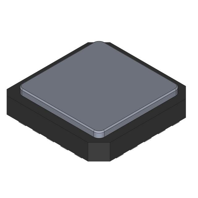
MAX9484ETP is housed in a 20-pin thin QFN package (4mm × 4mm) with exposed ground pad. Pin functions are electrically identical to MAX9485ETP per Maxim's documentation and pin compatibility assurance across the family.
| Pin/Terminal | Circuit Role | Design Meaning |
|---|---|---|
| VDD | Digital power supply | Bypassed with 0.1µF + 0.001µF to GND - powers digital logic, I²C interface, and output buffers |
| VDD_P | PLL analog power supply | Separate 3.3V rail bypassed to GND_P - isolates noise-sensitive PLL core from digital switching transients |
| GND / GND_P / EP | Ground terminals | Three dedicated ground connections - GND (digital), GND_P (PLL analog), EP (exposed pad, tied to GND) - minimize ground bounce and phase noise |
| X1 / X2 | Crystal oscillator terminals | Connect 27MHz fundamental-mode AT-cut crystal (±30ppm) - forms VCXO core with TUN voltage control |
| TUN | VCXO tuning voltage input | 0–3V analog control adjusts MCLK frequency ±200ppm - driven by MPEG processor DAC or filtered PWM |
| CLK_OUT1 / CLK_OUT2 | Programmable audio clock outputs | LVCMOS outputs (256/384/768×fS) - independently enabled/disabled; pulled low when disabled |
| MCLK | Buffered 27MHz master clock output | Direct VCXO output - used as reference for downstream PLLs or system timing; enabled via SAO1 (hardwire) or C7 bit (I²C) |
| MODE | Control interface selection | Low = I²C mode; High = hardwire mode - determines whether FS0/FS1/FS2 or SDA/SCL configure operation |
| RST | Asynchronous reset input | Active-low reset triggers 1024-cycle (37.7µs) initialization - restores default register state or hardwired configuration |
| SCL/FS0, SDA/FS1, FS2 | Multi-function control inputs | In I²C mode: SCL/SDA bus lines; in hardwire mode: three-level (low/high/open) sampling rate and scaling selectors |
| SAO1 / SAO2 | Address/config enable inputs | In I²C mode: set 7-bit slave address; in hardwire mode: control MCLK and CLK_OUT1/2 enable/disable states |
Key Features
| Feature | Design Value |
|---|---|
| Integrated VCXO with ±200ppm tuning | Eliminates need for external VCO or loop filter components - reduces BOM count and board area while enabling system clock lock |
| Two independent clock outputs with separate enables | Allows simultaneous generation of different audio clocks (e.g., front DAC @ 768×48kHz, surround DAC @ 384×96kHz) without inter-channel skew |
| No external PLL components required | Full PLL functionality (phase detector, loop filter, VCO, dividers) integrated - simplifies design validation and eliminates external component tolerances |
| I²C or hardwired configuration | Supports both firmware-driven flexibility (I²C) and fixed-function boot-time reliability (hardwire) - ideal for production variants and field-upgradable systems |
| 21ps RMS jitter at 73.728MHz | Meets stringent jitter requirements for 192kHz-equivalent audio paths - preserves dynamic range and minimizes THD+N in high-end DACs |
| 20-pin thin QFN (4mm × 4mm) | Reduces footprint by >40% vs. TSSOP - enables dense placement near audio codecs and minimizes trace length for jitter-sensitive signals |
Applications
| DVD Audio Subsystem | Digital HDTV Audio Processing |
|---|---|
Use Scenario: DVD player or drive extracts PCM audio data from MPEG-2 transport stream and routes it to dual-channel DACs for stereo playback. IC Role / Device Role / Timing Role: Generates synchronized 256×44.1kHz (11.2896MHz) and 384×48kHz (18.432MHz) clocks for left/right DACs while locking MCLK to system video timing via VCXO tuning. Use Value: Eliminates separate crystal oscillators per DAC channel, reduces EMI from multiple clock sources, and maintains <1ns inter-channel skew for coherent stereo imaging. |
Use Scenario: Digital HDTV receiver decodes multi-format audio (Dolby Digital, DTS) and drives discrete DACs for 5.1-channel surround sound. IC Role / Device Role / Timing Role: Provides 768×96kHz (73.728MHz) clock for high-resolution front channels and 384×44.1kHz (16.9344MHz) for center/rear channels, all derived from single 27MHz VCXO. Use Value: Ensures sample-accurate synchronization across six DACs using one timing source - prevents lip-sync drift and audio/video frame misalignment. |
| Set-Top Box Audio Output | Home Entertainment Center Sync |
Use Scenario: Cable/satellite STB outputs decoded audio via HDMI and SPDIF simultaneously while supporting legacy analog RCA outputs. IC Role / Device Role / Timing Role: Delivers 256×48kHz (12.288MHz) for HDMI audio PHY, 384×44.1kHz (16.9344MHz) for SPDIF transmitter, and 27MHz MCLK for system SoC interface. Use Value: Enables concurrent multi-interface audio output without clock domain crossing logic - avoids sample rate conversion artifacts and buffer underruns. |
Use Scenario: AV receiver integrates Blu-ray player, streaming box, and game console, requiring unified audio clocking across all sources. IC Role / Device Role / Timing Role: Acts as central audio clock hub - accepts 27MHz reference from primary source and regenerates clean, jitter-reduced clocks for all connected devices via VCXO lock. Use Value: Removes clock source dependency between subsystems - allows seamless source switching without audible click/pop from clock resynchronization. |
Equivalent & Alternatives
The following parts are listed as comparable options for similar programmable audio clock generator applications.
| Alternative Part | Technical Difference | Application Difference | Selection Advice |
|---|---|---|---|
| MAX9485ETP | Identical pinout, electrical specs, and functional block diagram; documented as direct replacement in Maxim's ordering matrix | Same MPEG-2 audio clocking use cases; validated in identical reference designs (e.g., MAX9485EVKIT) | Select MAX9485ETP when full documentation, evaluation kit support, and long-term Maxim product continuity are prioritized |
| Si5338A-D-GM | Wider frequency range (0.16–350MHz), I²C + SPI interface, but higher typical jitter (35ps RMS at 73.728MHz) and no integrated VCXO | Requires external VCXO or crystal + tuning circuit for system lock; suited for multi-protocol timing (audio + video + data) | Choose Si5338A-D-GM only if needing non-audio frequencies or multi-protocol flexibility - not drop-in for VCXO-dependent MPEG-2 sync |
Compared with MAX9485ETP, the MAX9484ETP shares identical timing performance and pin compatibility but may reflect a factory-trimmed variant optimized for specific production lots; versus Si5338A-D-GM, it trades broader programmability for lower jitter, integrated VCXO, and simpler audio-specific configuration - making it superior for cost-sensitive, high-fidelity MPEG-2 audio systems.
Availability
MAX9484ETP is available at Aetrix Electronics and suitable for DVD players, digital HDTV receivers, and set-top boxes requiring stable component supply, low-jitter audio clocking, and industrial temperature operation.
Supply support for MAX9484ETP includes scheduled delivery planning, volume procurement assistance, BOM continuity management, traceable sourcing, and lifecycle availability coordination for OEM customers, industrial embedded developers, connected-device designers, and electronics production programs.
Manufacturer
Maxim Integrated (now part of Analog Devices) is a semiconductor company specializing in precision analog, mixed-signal, and power management ICs for industrial, communications, and consumer applications.
The MAX9484ETP belongs to Maxim's audio timing product line, engineered specifically to replace discrete crystal oscillators and PLLs in MPEG-2 audio decoding systems - delivering low-jitter, multi-output clock generation with system-level VCXO synchronization.
FAQ
What is the function of the TUN pin on the MAX9484ETP?
The TUN pin on the MAX9484ETP is the voltage-controlled tuning input for the integrated VCXO. Applying a DC voltage from 0V to 3V adjusts the 27MHz MCLK output frequency over a ±200ppm range, enabling precise alignment with the host MPEG processor's system clock. This eliminates the need for external tuning components and ensures robust audio-video synchronization in real-time decoding systems. The MAX9484ETP's TUN input has 94kΩ impedance and responds within 10µs to voltage changes.
Does the MAX9484ETP support both I²C and hardwired configuration simultaneously?
No, the MAX9484ETP does not support simultaneous I²C and hardwired configuration. The MODE pin selects one exclusive mode: when MODE is low, SCL/FS0 and SDA/FS1 operate as I²C bus lines, and FS2 is ignored; when MODE is high, those pins become three-level function selection inputs (FS0/FS1/FS2), and I²C communication is disabled. This hardware-muxed design prevents bus contention and ensures deterministic startup behavior in the MAX9484ETP.
What is the maximum output frequency achievable with the MAX9484ETP?
The MAX9484ETP achieves a maximum output frequency of 73.728MHz, realized when configured for 768×fS with fS = 96kHz. This frequency is fully supported across the −40°C to +85°C operating range and exhibits 21ps RMS period jitter under typical conditions (VDD = 3.3V, CL = 20pF). The MAX9484ETP's output drivers maintain 45–55% duty cycle and ≤2ns rise/fall times at this frequency, meeting LVCMOS timing requirements for high-speed audio interfaces.
How does the MAX9484ETP handle power-on reset and external reset?
The MAX9484ETP incorporates an internal power-on reset that activates when VDD exceeds 2.2V and completes after 1024 cycles of the 27MHz reference clock (~37.7µs). An external reset is triggered by driving the RST pin low for >20ns, also requiring 1024 reference cycles to complete. During reset, the MAX9484ETP initializes registers to defaults: in I²C mode, CLK_OUT1/2 = 256×32kHz; in hardwire mode, outputs follow FS0/FS1/FS2 states. RST is internally pulled high, so no external pull-up is required.
Can the MAX9484ETP generate different frequencies on CLK_OUT1 and CLK_OUT2 simultaneously?
Yes, the MAX9484ETP can generate different frequencies on CLK_OUT1 and CLK_OUT2 simultaneously. Each output is independently configurable for scaling factor (256/384/768×fS) and sampling frequency (12–96kHz) via either I²C register bits (C2–C0 for CLK_OUT1, C3–C1 for CLK_OUT2) or hardwired inputs (FS0/FS1/FS2 plus SAO1/SAO2 enable logic). This allows, for example, CLK_OUT1 = 768×48kHz (36.864MHz) for a front DAC and CLK_OUT2 = 384×96kHz (36.864MHz) for a subwoofer DAC - both at identical frequency but with independent enable control in the MAX9484ETP.
MAX9484ETP Specifications
- Product attributes
- Attribute value
- Manufacturer:
- Analog Devices Inc./Maxim Integrated
- Series:
- *
- Package/Case:
- -
- Packaging:
- Bulk
- Product Status:
- Active
- Type:
- -
- Data Rate:
- -
- Number of Channels:
- -
- Voltage - Supply:
- -
- Current - Supply:
- -
- Current - Modulation:
- -
- Current - Bias:
- -
- Operating Temperature:
- -
- Grade:
- -
- Qualification:
- -
- Supplier Device Package:
- -
- Mounting Type:
- -
MAX9484ETP FAQ
1.How can I place an order for MAX9484ETP through Aetrix?
Please submit a Request for Quotation (RFQ) for MAX9484ETP on Aetrix. Our sales agent will provide a competitive quotation and guide you through the order confirmation once you accept the terms.
2.Are the price and stock information for MAX9484ETP reliable?
The price and inventory of MAX9484ETP are updated periodically and may fluctuate due to market conditions. Stock and pricing data are typically refreshed every 24 hours. Quotation validity for MAX9484ETP is usually 5 days.
3.What payment methods are accepted for MAX9484ETP?
We accept Wire Transfer, PayPal, Credit Card, Western Union, MoneyGram, and Escrow for MAX9484ETP transactions.
Note: Certain payment methods may incur a processing fee.
4.How is shipping managed for MAX9484ETP?
MAX9484ETP orders can be shipped via leading logistics carriers, including DHL, UPS, FedEx, TNT, or Registered Mail.
Once your MAX9484ETP order is processed, you will receive an email with the shipment details and tracking number.
Note: Tracking information may take up to 24 hours to appear. Express delivery typically takes 3–5 business days.
5.How can I obtain technical support or documentation for MAX9484ETP?
For technical support, including MAX9484ETP datasheets, pinout diagrams, or application guidance, please contact our engineering support team. They can provide detailed documentation and assistance for your MAX9484ETP requirements.
6.How does Aetrix verify that MAX9484ETP is sourced from the original manufacturer or authorized distributors?
All MAX9484ETP products on Aetrix are procured from qualified distributors and authorized channels. Our dedicated quality assurance team conducts strict verification, including traceability checks and, if necessary, third-party testing. This ensures that MAX9484ETP meets industry standards.
7.What is the process for return or replacement of MAX9484ETP?
All MAX9484ETP units undergo pre-shipment inspection (PSI). If there is an issue with MAX9484ETP, returns or replacements are accepted under the following conditions:
1.Quantity discrepancies, incorrect items, or visible external defects (such as breakage or corrosion), acknowledged by Aetrix.
2.The issue is reported within 90 days of delivery.
3.The MAX9484ETP part is unused and in its original packaging.
Return procedure for MAX9484ETP:
1.Submit a request within 90 days.
2.Obtain a Return Material Authorization (RMA) from Aetrix.
MAX9484ETP Tags
-
EPC21701
EPC
-
EPC21601
EPC
-
MAX3799ETJ+T
Analog Devices Inc./Maxim Integrated
-
AD9665ACPZ-REEL7
Analog Devices Inc.

-
MAX3740AETG+T
Analog Devices Inc./Maxim Integrated
-
MAX3795ETG+
Analog Devices Inc./Maxim Integrated

-
EPC21603
EPC
-
ONET8501VRGPT
Texas Instruments
-
MAX3738ETG+T
Analog Devices Inc./Maxim Integrated
-
SY88022ALMG-TR
Microchip Technology
-
ISL78365ARZ-T7A
Renesas
-
EPC21603ENGRT
EPC
Tech Hub

A practical engineering guide to 3.3V and 5V logic compatibility, input thresholds, resistor dividers, translator ICs, MOSFET level shifting, I2C pull-ups, timing limits and power-sequencing risks.

The 74HC595 uses push-pull logic outputs, while the TPIC6B595 uses 50 V open-drain DMOS sinks for higher-power loads. This guide compares timing, current limits, 3.3 V interfacing, load wiring, thermal…

The 74HC595 converts serial data into eight stable parallel outputs. This guide covers pin functions, shift and storage timing, OE and MR behavior, drive-current limits, cascading, voltage compatibilit…

A technical comparison of level-sensitive latches and edge-triggered flip-flops, covering timing windows, setup and hold limits, master–slave operation, time borrowing, race-through, HDL inference and…

A D latch stores one bit while Enable controls when data can pass. This reference covers gate-level operation, truth tables, transparency, setup and hold timing, LE versus OE, common ICs and practical …

An SR latch stores one bit through cross-coupled feedback. This engineering reference covers NOR and NAND implementations, truth tables, forbidden-state recovery, gated operation, switch debouncing, fa…

Latch circuits retain one bit through feedback. This technical reference covers SR and D latches, truth tables, transparency, timing limits, latch-versus-flip-flop behavior, applications and common log…

An engineering guide to LED driver operation, constant-current and constant-voltage outputs, linear and switching topologies, dimming, IC selection, calculations, replacement compatibility, and fault c…

Operational amplifier guide covering op amp basics, feedback, ideal vs real op amps, common configurations, buffer circuits, offset, bias current, gain-bandwidth, slew rate, rail-to-rail limits and sel…

Jumper cables guide covering safe connection order, red and black clamp placement, final ground connection, cable gauge, length, clamp quality, copper vs CCA cables, jump starter comparison and battery…


