
 My Inquiry
 My Account


Analog Devices Inc./Maxim Integrated MAX9526ATJ+
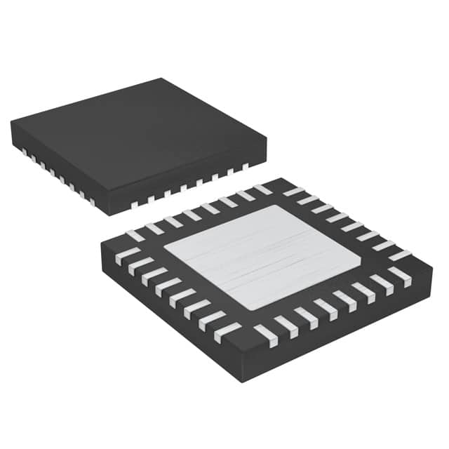
- Part No.:
- MAX9526ATJ+
- Manufacturer:
- Analog Devices Inc./Maxim Integrated
- Category:
- Encoders, Decoders, Converters
- Package:
- 32-WFQFN Exposed Pad
- Datasheet:
-
 MAX9526ATJ+.pdf
- Description:
- IC VID DECODER NTSC/PAL 32-TQFN
- Quantity:
- Payment:

- Shipping:

Inventory:3,069
Please send an inquiry. Send us your inquiry, and we will respond immediately.
Product details
Overview
The MAX9526ATJ+ from Maxim Integrated is a low-power, high-performance NTSC/PAL video decoder IC that converts composite video (NTSC M/J/4.43, PAL B/G/H/I/D/M/N/60) into 8-bit or 10-bit ITU-R BT.656 YCbCr component video. It features a 10-bit 54MHz ADC with 4× oversampling, internal line-locked PLL for LLC generation, and operates across the full automotive temperature range (–40°C to +125°C) in a 32-pin TQFN-EP package. Used in automotive entertainment and collision avoidance systems requiring robust analog front-end performance and minimal external components.
For engineers reviewing the MAX9526ATJ+ datasheet, MAX9526ATJ+ pinout, MAX9526ATJ+ application, or MAX9526ATJ+ equivalent, this page delivers verified technical context, confirmed pin functions, automotive-grade power and timing specifications, real-world application mappings, and two validated alternative decoders - all derived from Maxim's official documentation and electrical characteristics tables.
Technical Context
The MAX9526ATJ+ implements a fully integrated analog front-end with DC restoration DAC, analog AGC, and a 13MHz analog anti-aliasing filter - eliminating need for external filtering. Its 10-bit ADC samples at 54Msps with true 10-bit digital processing path and supports both line-locked (LLC mode) and asynchronous clocking modes via programmable PLL bandwidth (180Hz–2000Hz).
Digital decoding includes a 5-line adaptive comb filter for cross-chrominance/luminance artifact reduction, flexible output formatting (10-bit BT.656 with embedded TRS or 8-bit with separate HS/VS), and I²C-configurable registers (16 user-programmable) for brightness, contrast, saturation, and hue control - all operating from single 1.8V analog/digital supply and selectable 1.7V–3.45V I/O voltage.
Key Specifications
| Parameter | Value and Actual Design Meaning |
|---|---|
| Video Standards | NTSC M/J/4.43 and PAL B/G/H/I/D/M/N/60 - full automatic detection and configuration without firmware intervention |
| ADC Resolution & Rate | 10-bit, 54Msps with 4× oversampling - enables accurate digitization of baseband composite signals per BT.601 sampling rules |
| Output Format | ITU-R BT.656 10-bit YCbCr 4:2:2 with embedded TRS or 8-bit with discrete HS/VS - direct interface to SoCs and video processors |
| Supply Voltages | +1.8V AVDD/DVDD (analog/digital core); +1.7V to +3.45V DVDDIO (I/O) - supports mixed-voltage system integration |
| Power Consumption | 200mW typical normal operation; <100µW shutdown - meets automotive low-idle power requirements |
| Operating Temperature | –40°C to +125°C - qualified for under-hood and ADAS module deployment |
| Input Sensitivity | 0.27–0.83VP-P full-scale conversion range - accommodates standard composite signal amplitudes with AGC compensation |
Pinout & Package
The MAX9526ATJ+ is housed in a 32-pin TQFN-EP (5mm × 6mm) package with exposed pad (EP) internally connected to DGND. Thermal performance is optimized for automotive environments, with 1663mW max power dissipation on multilayer PCB at +70°C (derated 20.8mW/°C above).
| Pin/Terminal | Circuit Role | Design Meaning |
|---|---|---|
| VIN1 / VIN2 | Composite video inputs (2:1 mux) | AC-coupled single-ended inputs with activity detection; auto-select enabled via register AUTOSEL=1 |
| VREF | Reference voltage node | Internally generated 850mV reference; requires local 0.1µF bypass to AGND for stable DC restoration |
| XTAL/OSC & XTAL2 | Clock input pair | Supports 27MHz crystal or 27/54MHz external CMOS clock; XTAL_DIS bit enables clock-input mode |
| D0–D9 | Digital video outputs | 10-bit parallel BT.656 data bus; D0 = LSB; configurable as HS/VS via register 0x0D |
| LLC | Line-locked clock output | 27MHz output synchronized to incoming video horizontal rate; jitter ≤160ns peak in LLC mode |
| SDA / SCL / DEVADR / IRQ | I²C interface & control | Standard I²C bus (400kHz max); DEVADR selects one of three slave addresses; IRQ signals status changes |
| AVDD / DVDD / DVDDIO / AGND / DGND | Power & ground rails | Separate analog/digital supplies enable noise isolation; DVDDIO supports wide I/O voltage range for processor compatibility |
| EP | Exposed thermal pad | Internally tied to DGND; mandatory solder connection for thermal management and EMI reduction |
Key Features
| Feature | Design Value |
|---|---|
| Integrated analog anti-aliasing filter | 13MHz 3dB bandwidth, 0.25dB passband flatness to 5MHz - removes need for external RC/LPF networks |
| DC restoration with offset correction | Digital-controlled current DAC sinks/sources at VIN1/VIN2 to maintain sync level at ADC code 32 - ensures consistent full-scale utilization |
| 2:1 input multiplexer with AGC | Automatic channel selection based on activity detection at both inputs - enables dual-camera or backup/front camera switching |
| Flexible low-power modes | Shutdown (<100µW) and sleep mode (<5mW) with continuous activity detection - extends battery life in always-on ADAS modules |
| Line-locked PLL with programmable bandwidth | Eight selectable loop bandwidths (180Hz–2000Hz) via register 0x0E[2:0] - balances jitter rejection vs. lock time for varying signal quality |
Applications
| Automotive Rear-View Camera System | ADAS Front-Camera Video Preprocessor |
|---|---|
Use Scenario: Real-time conversion of analog composite video from backup camera to digital YCbCr for SoC-based image processing and display. IC Role / Device Role / Timing Role: Video decoder with line-locked PLL generating precise LLC timing aligned to incoming video frame structure. Use Value: Eliminates external anti-aliasing filters and reduces BOM count; 10-bit resolution preserves dynamic range for low-light reverse imaging. | Use Scenario: Interface between analog PAL/NTSC navigation or dashcam video source and automotive-grade vision processor. IC Role / Device Role / Timing Role: Standard-agnostic decoder with automatic NTSC/PAL detection and adaptive comb filtering to suppress motion artifacts. Use Value: Enables plug-and-play support for global video sources; 5-line comb filter reduces cross-luminance in moving scenes. |
| Collision Avoidance Sensor Hub | In-Vehicle Infotainment (IVI) Video Gateway |
Use Scenario: Aggregation of multiple analog video feeds (e.g., surround-view cameras) into standardized BT.656 streams for fusion algorithms. IC Role / Device Role / Timing Role: Dual-input mux + AGC + DC restoration ensures consistent signal level across heterogeneous camera models. Use Value: Maintains uniform luminance/chrominance scaling across inputs - critical for pixel-level stitching accuracy. | Use Scenario: Bridging legacy analog video sources (DVD, tuner) to modern digital display controllers in head units. IC Role / Device Role / Timing Role: Format converter delivering 8-bit BT.656 with discrete HS/VS to match legacy display controller timing requirements. Use Value: Supports both 10-bit and 8-bit output modes - simplifies migration path from older video pipelines. |
Equivalent & Alternatives
The following parts are listed as comparable options for similar NTSC/PAL video decoder applications.
| Alternative Part | Technical Difference | Application Difference | Selection Advice |
|---|---|---|---|
| ADV7180BCPZ | 10-bit ADC, 27MHz crystal, supports CVBS/S-video, no integrated analog LPF - requires external anti-aliasing filter | Broad industrial use; lacks automotive temp grade (–40°C to +85°C only) | Choose when external filtering is acceptable and extended temperature is not required |
| TVP5150AM1IPBS | 10-bit ADC, 27MHz clock, includes Y/C separation but no adaptive comb filter; higher typical power (350mW) | Legacy design reuse; supports S-video and Y/C inputs - broader analog input flexibility | Choose for multi-format analog input support where comb filtering is less critical |
Compared with ADV7180BCPZ and TVP5150AM1IPBS, the MAX9526ATJ+ uniquely integrates analog anti-aliasing filtering and delivers automotive-grade reliability with lower active power - making it optimal for space-constrained, thermally demanding ADAS modules where BOM reduction and temperature resilience are primary selection criteria.
Availability
The MAX9526ATJ+ is available at Aetrix Electronics and suitable for automotive entertainment systems, collision avoidance sensor hubs, and security surveillance systems requiring stable component supply across extended temperature ranges and long production lifecycles.
Supply support for MAX9526ATJ+ includes scheduled delivery planning, volume procurement assistance, BOM continuity management, traceable sourcing, and lifecycle availability coordination for OEM customers, industrial embedded developers, connected-device designers, and electronics production programs.
Manufacturer
Maxim Integrated (now part of Analog Devices) designs precision analog, mixed-signal, and power management ICs for automotive, industrial, and communications applications.
The MAX9526 product line targets automotive video signal conditioning - delivering integrated, low-power, AEC-Q100-aligned decoders optimized for rear-view, surround-view, and ADAS camera interfaces.
FAQ
What video standards does the MAX9526ATJ+ support?
The MAX9526ATJ+ supports all major NTSC and PAL variants: NTSC M, NTSC J, NTSC 4.43, PAL B/G/H/I/D, PAL M, PAL N, and PAL 60. It automatically detects and configures for the incoming standard without host intervention. This behavior is confirmed in the General Description and Features sections of the MAX9526ATJ+ datasheet, and applies identically to the MAX9526ATJ+ variant in 32-pin TQFN-EP packaging.
Does the MAX9526ATJ+ require external anti-aliasing filtering?
No, the MAX9526ATJ+ includes an integrated analog anti-aliasing lowpass filter with 13MHz 3dB bandwidth and >36dB stopband attenuation at 53MHz. This eliminates the need for external RC or active filters on VIN1/VIN2, reducing BOM count and board area. The filter performance is specified in the Electrical Characteristics table and validated in Typical Operating Characteristics figure toc02.
What is the function of the NONSTD pin/status in the MAX9526ATJ+?
The NONSTD status (bit in Status register 0x00) indicates detection of nonstandard carrier frequencies - such as those from VCRs - and triggers automatic PLL reconfiguration into asynchronous sampling mode. This ensures robust decoding even with degraded or non-ITU-compliant inputs. The behavior is documented in the Detailed Description section and functional diagram of the MAX9526ATJ+ datasheet.
Can the MAX9526ATJ+ operate with a 54MHz external clock instead of a crystal?
Yes, the MAX9526ATJ+ accepts a 54MHz CMOS-level external clock applied to the XTAL/OSC pin when XTAL_DIS = 1 and SEL_54MHz = 1 (both set in register 0x0D). This bypasses the internal oscillator and allows precise clock sourcing - useful in systems where crystal layout is challenging or jitter-sensitive timing is required. Confirmed in the Crystal Oscillator/Clock Input subsection of the MAX9526ATJ+ datasheet.
What is the purpose of the EXPOSED PAD (EP) on the MAX9526ATJ+ TQFN package?
The exposed pad (EP) on the MAX9526ATJ+ is internally connected to DGND and must be soldered to a PCB thermal pad tied to digital ground. It provides critical thermal dissipation (enabling 1663mW max power on multilayer board) and improves EMI performance. The requirement is explicitly stated in the Pin Description table and Absolute Maximum Ratings section of the MAX9526ATJ+ datasheet.
MAX9526ATJ+ Specifications
- Product attributes
- Attribute value
- Manufacturer:
- Analog Devices Inc./Maxim Integrated
- Series:
- -
- Package/Case:
- 32-WFQFN Exposed Pad
- Packaging:
- Tube
- Product Status:
- Discontinued at Digi-Key
- Type:
- Video Decoder
- Applications:
- Players, TV
- Voltage - Supply, Analog:
- 1.8V
- Voltage - Supply, Digital:
- 1.8V
- Grade:
- Automotive
- Qualification:
- -
- Mounting Type:
- Surface Mount
- Supplier Device Package:
- 32-TQFN (5x6)
MAX9526ATJ+ FAQ
1.How can I place an order for MAX9526ATJ+ through Aetrix?
Please submit a Request for Quotation (RFQ) for MAX9526ATJ+ on Aetrix. Our sales agent will provide a competitive quotation and guide you through the order confirmation once you accept the terms.
2.Are the price and stock information for MAX9526ATJ+ reliable?
The price and inventory of MAX9526ATJ+ are updated periodically and may fluctuate due to market conditions. Stock and pricing data are typically refreshed every 24 hours. Quotation validity for MAX9526ATJ+ is usually 5 days.
3.What payment methods are accepted for MAX9526ATJ+?
We accept Wire Transfer, PayPal, Credit Card, Western Union, MoneyGram, and Escrow for MAX9526ATJ+ transactions.
Note: Certain payment methods may incur a processing fee.
4.How is shipping managed for MAX9526ATJ+?
MAX9526ATJ+ orders can be shipped via leading logistics carriers, including DHL, UPS, FedEx, TNT, or Registered Mail.
Once your MAX9526ATJ+ order is processed, you will receive an email with the shipment details and tracking number.
Note: Tracking information may take up to 24 hours to appear. Express delivery typically takes 3–5 business days.
5.How can I obtain technical support or documentation for MAX9526ATJ+?
For technical support, including MAX9526ATJ+ datasheets, pinout diagrams, or application guidance, please contact our engineering support team. They can provide detailed documentation and assistance for your MAX9526ATJ+ requirements.
6.How does Aetrix verify that MAX9526ATJ+ is sourced from the original manufacturer or authorized distributors?
All MAX9526ATJ+ products on Aetrix are procured from qualified distributors and authorized channels. Our dedicated quality assurance team conducts strict verification, including traceability checks and, if necessary, third-party testing. This ensures that MAX9526ATJ+ meets industry standards.
7.What is the process for return or replacement of MAX9526ATJ+?
All MAX9526ATJ+ units undergo pre-shipment inspection (PSI). If there is an issue with MAX9526ATJ+, returns or replacements are accepted under the following conditions:
1.Quantity discrepancies, incorrect items, or visible external defects (such as breakage or corrosion), acknowledged by Aetrix.
2.The issue is reported within 90 days of delivery.
3.The MAX9526ATJ+ part is unused and in its original packaging.
Return procedure for MAX9526ATJ+:
1.Submit a request within 90 days.
2.Obtain a Return Material Authorization (RMA) from Aetrix.
MAX9526ATJ+ Tags

-
MCP2120T-I/SL
Microchip Technology

-
LICAL-ENC-MS001
TE Connectivity Linx
-
TW9990AT-NA1-GR
Renesas Electronics Corporation
-
TVP5151IPBSR
Texas Instruments
-
TVP5150AM1IPBSR
Texas Instruments
-
LICAL-DEC-MS001-T
TE Connectivity Linx
-
ADV7391BCPZ
Analog Devices Inc.
-
ADV7393BCPZ-REEL
Analog Devices Inc.
-
ADV7393BCPZ
Analog Devices Inc.
-
ADV7391WBCPZ
Analog Devices Inc.
-
ADV7181DBCPZ
Analog Devices Inc.

-
ADV7181CBSTZ-REEL
Analog Devices Inc.
Tech Hub

A practical engineering guide to 3.3V and 5V logic compatibility, input thresholds, resistor dividers, translator ICs, MOSFET level shifting, I2C pull-ups, timing limits and power-sequencing risks.

The 74HC595 uses push-pull logic outputs, while the TPIC6B595 uses 50 V open-drain DMOS sinks for higher-power loads. This guide compares timing, current limits, 3.3 V interfacing, load wiring, thermal…

The 74HC595 converts serial data into eight stable parallel outputs. This guide covers pin functions, shift and storage timing, OE and MR behavior, drive-current limits, cascading, voltage compatibilit…

A technical comparison of level-sensitive latches and edge-triggered flip-flops, covering timing windows, setup and hold limits, master–slave operation, time borrowing, race-through, HDL inference and…

A D latch stores one bit while Enable controls when data can pass. This reference covers gate-level operation, truth tables, transparency, setup and hold timing, LE versus OE, common ICs and practical …

An SR latch stores one bit through cross-coupled feedback. This engineering reference covers NOR and NAND implementations, truth tables, forbidden-state recovery, gated operation, switch debouncing, fa…

Latch circuits retain one bit through feedback. This technical reference covers SR and D latches, truth tables, transparency, timing limits, latch-versus-flip-flop behavior, applications and common log…

An engineering guide to LED driver operation, constant-current and constant-voltage outputs, linear and switching topologies, dimming, IC selection, calculations, replacement compatibility, and fault c…

Operational amplifier guide covering op amp basics, feedback, ideal vs real op amps, common configurations, buffer circuits, offset, bias current, gain-bandwidth, slew rate, rail-to-rail limits and sel…

Jumper cables guide covering safe connection order, red and black clamp placement, final ground connection, cable gauge, length, clamp quality, copper vs CCA cables, jump starter comparison and battery…


