
 My Inquiry
 My Account


Analog Devices Inc./Maxim Integrated MAX9532AUB/V+T
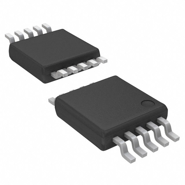
- Part No.:
- MAX9532AUB/V+T
- Manufacturer:
- Analog Devices Inc./Maxim Integrated
- Category:
- Video Amps and Modules
- Package:
- 10-TFSOP, 10-MSOP (0.118", 3.00mm Width)
- Datasheet:
-
 MAX9532AUB/V+T.pdf
- Description:
- IC POWER MANAGEMENT
- Quantity:
- Payment:

- Shipping:

Inventory:30,000
Please send an inquiry. Send us your inquiry, and we will respond immediately.
Product details
Overview
The MAX9532AUB/V+T from Maxim Integrated is a DirectDrive® video filter amplifier designed for automotive infotainment systems, featuring integrated short-to-battery protection (up to 18V), 4V/V fixed gain, DC-coupled input/output, and an internal 5-pole Butterworth reconstruction filter with ±1dB passband flatness to 9.5MHz.
For engineers reviewing the MAX9532AUB/V+T datasheet, MAX9532AUB/V+T pinout, MAX9532AUB/V+T application, or MAX9532AUB/V+T equivalent, this page delivers verified technical context, validated pin functions, automotive-grade thermal performance (-40°C to +125°C), and real-world design meaning behind key specs including charge-pump noise suppression, sync-tip clamping, and battery-short response timing.
Technical Context
The MAX9532AUB/V+T implements a fully integrated DirectDrive architecture: an internal charge pump (220–660kHz switching) and linear regulator generate a clean negative supply (CPVSS) enabling true ground-referenced black level and sync pulses below ground without external capacitors. Its 5-pole Butterworth lowpass filter ensures ±1dB gain flatness up to 9.5MHz and 42dB attenuation at 27MHz.
Short-to-battery protection operates via a dedicated JACKSENSE input monitoring output connector voltage; detection of >8V triggers internal switch disablement within 10µs, isolating the amplifier from faults up to 18V. The transparent sync-tip clamp supports both AC- and DC-coupled inputs by applying ≤3.3µA clamping current only when needed.
Key Specifications
| Parameter | Value and Actual Design Meaning |
|---|---|
| Supply Voltage | 3.0V to 3.6V single supply - enables direct interface with 3.3V automotive domain controllers without level-shifting. |
| Fixed Gain | 4V/V (3.92–4.08V/V over temp) - delivers nominal 2VP-P output from 0.5VP-P DAC input, matching standard composite video drive requirements. |
| Reconstruction Filter | 5-pole Butterworth, ±1dB flatness to 9.5MHz - preserves NTSC/PAL luminance/chroma integrity and suppresses DAC imaging artifacts. |
| Short-to-Battery Threshold | 8.0V ±0.7V - reliably distinguishes battery faults from normal load transients in 12V automotive systems. |
| Output Disconnect Time | 20µs max - prevents latch-up or thermal damage during fast-rising battery shorts (e.g., connector mating). |
| Differential Gain/Phase | 0.7% / 0.5° @ 4.43MHz - meets broadcast-grade video fidelity for rear-seat displays and camera feeds. |
| Quiescent Current | 15–23mA - enables low-power operation in always-on infotainment modules without thermal derating. |
Pinout & Package
The MAX9532AUB/V+T is housed in a 3mm × 3mm, 10-pin µMAX® package rated for -40°C to +125°C operation, optimized for space-constrained automotive PCB layouts with exposed pad thermal enhancement.
| Pin/Terminal | Circuit Role | Design Meaning |
|---|---|---|
| 1 VDD | Positive power supply input | Bypassed with 1µF capacitor to GND; supplies all internal circuitry including charge pump and amplifier core. |
| 2 C1P | Charge-pump flying capacitor positive terminal | Connects to one end of 1µF ceramic flying cap; forms switched-capacitor inverter stage for CPVSS generation. |
| 3 CPGND | Charge-pump ground reference | Must be tied directly to system GND; provides stable return for charge-pump switching currents. |
| 4 C1N | Charge-pump flying capacitor negative terminal | Connects to other end of 1µF flying cap; completes charge-transfer path for negative voltage synthesis. |
| 5 CPVSS | Charge-pump negative output supply | Bypassed with 1µF || 10nF to GND; powers amplifier output stage to enable sync-tip drive below ground. |
| 6 VSS | Negative power supply rail | Internally connected to CPVSS; must be externally tied to CPVSS pin for proper biasing. |
| 7 OUT | Filtered video output | Drives 75Ω or 100Ω loads directly; integrates short-to-battery protection switch in series with output path. |
| 8 JACKSENSE | Battery fault detection input | Monitors output connector voltage; triggers protection when >8V detected, enabling fail-safe disconnection. |
| 9 GND | Analog ground reference | Primary signal return; must be star-connected to minimize noise coupling into video path. |
| 10 IN | Video input | Accepts 0.5VP-P full-scale signals; includes transparent sync-tip clamp for AC-coupled sources. |
Key Features
| Feature | Design Value |
|---|---|
| DirectDrive® architecture | Eliminates 220–3000µF DC-blocking capacitors at output, reducing board area by >80% and eliminating sag distortion in fast-changing video scenes. |
| Integrated short-to-battery protection | Withstands 18V battery shorts without external components; disconnects output in 20µs to prevent latch-up or thermal failure in vehicle harness faults. |
| Transparent sync-tip clamp | Applies ≤3.3µA clamping current only during AC-coupled input undershoot, preserving DC accuracy for DC-coupled sources while enabling legacy interface compatibility. |
| Automotive temperature range | Specified from -40°C to +125°C ambient - qualified per AEC-Q100 requirements for under-dash and head-unit mounting locations. |
| Low-glitch charge pump | Injects ≤40pVs glitch impulse at output - ensures visibly flawless video without visible noise bars or sync jitter in high-resolution displays. |
Applications
| Rear-View Camera Display | Dashboard Video Infotainment |
|---|---|
|
Use Scenario: Driving video signal from CMOS image sensor through long cable to LCD display in rear-view mirror module. IC Role / Device Role / Timing Role: Video filter amplifier with reconstruction filtering, DC-level shifting, and short-circuit protection on output trace routed near vehicle chassis. Use Value: DirectDrive eliminates bulky output capacitors, enabling ultra-thin mirror housing; short-to-battery protection survives accidental grounding of RCA connector to 12V chassis. |
Use Scenario: Processing composite video from navigation ASIC for overlay on instrument cluster TFT display. IC Role / Device Role / Timing Role: Final-stage video driver with precise black-level control and sync-tip integrity for real-time graphics overlay. Use Value: ±1dB gain flatness to 9.5MHz preserves sharp text edges in map overlays; 0.5° differential phase minimizes color fringing at icon boundaries. |
| Backup Camera System ECU | Head-Unit Video Pass-Through |
|
Use Scenario: Integrating analog video input from multiple cameras into central processing unit with hot-swap capability. IC Role / Device Role / Timing Role: Input conditioning and fault-isolated video buffer with jack-sense–enabled short detection before signal routing. Use Value: JACKSENSE input detects connector insertion/removal events and disables output during mating to prevent arcing; 10ms recovery ensures seamless video resumption. |
Use Scenario: Passing composite video from HDMI-to-analog converter to legacy rear-seat entertainment display. IC Role / Device Role / Timing Role: Signal integrity conditioner compensating for DAC quantization steps and cable-induced high-frequency loss. Use Value: 42dB attenuation at 27MHz suppresses sampling clock harmonics that cause beat patterns on large-screen displays; 0.1% nonlinearity prevents gradient banding. |
Equivalent & Alternatives
The following parts are listed as comparable options for similar video filter amplifier applications.
| Alternative Part | Technical Difference | Application Difference | Selection Advice |
|---|---|---|---|
| MAX9531AUB/V+T | Same package and temperature grade, but lacks short-to-battery protection and uses external negative supply instead of DirectDrive. | Requires dual supply and external -3.3V rail; unsuitable for battery-short–prone environments like trunk-mounted cameras. | Select MAX9531AUB/V+T only if system already provides clean negative rail and short-to-battery risk is mitigated externally. |
| THS7374IPWPR | 4-channel, 3.3V video amplifier with 10MHz bandwidth and no integrated reconstruction filter or short-to-battery protection. | Needs external RC filter for DAC reconstruction; lacks automotive fault tolerance and requires separate protection circuitry. | Choose THS7374IPWPR for multi-channel cost-sensitive designs where DirectDrive and fault protection are not required. |
Compared with MAX9531AUB/V+T and THS7374IPWPR, the MAX9532AUB/V+T uniquely combines single-supply DirectDrive operation, integrated 9.5MHz reconstruction filtering, and automotive-grade short-to-battery resilience - eliminating four external components and enabling robust, space-efficient video routing in safety-critical automotive zones.
Availability
The MAX9532AUB/V+T is available at Aetrix Electronics and suitable for automotive infotainment systems, rear-view camera modules, and dashboard video displays requiring stable component supply across extended temperature ranges and long production lifecycles.
Supply support for MAX9532AUB/V+T includes scheduled delivery planning, volume procurement assistance, BOM continuity management, traceable sourcing, and lifecycle availability coordination for OEM customers, industrial embedded developers, connected-device designers, and electronics production programs.
Manufacturer
Maxim Integrated (now part of Analog Devices) is a U.S.-based semiconductor company specializing in high-performance analog, mixed-signal, and power management ICs for automotive, industrial, and communications markets.
The MAX9532AUB/V+T belongs to Maxim's DirectDrive video amplifier product line, engineered specifically for automotive video signal conditioning where space, reliability, and fault tolerance are critical in harsh electrical environments.
FAQ
What is the primary function of the JACKSENSE pin on the MAX9532AUB/V+T?
The JACKSENSE pin on the MAX9532AUB/V+T monitors the voltage at the video output connector to detect short-to-battery faults. When it senses >8V (±0.7V), it triggers internal switch disablement within 20µs, protecting the MAX9532AUB/V+T from damage during automotive wiring faults. It is not a general-purpose input and must be connected after the back-termination resistor per the datasheet layout guidelines.
Does the MAX9532AUB/V+T require external capacitors for its charge pump?
Yes, the MAX9532AUB/V+T requires two external 1µF ceramic capacitors: one between C1P and C1N (pins 2 and 4) for charge transfer, and another between CPVSS and GND (pin 5) for noise filtering. These are mandatory for DirectDrive operation; omitting them prevents negative supply generation and causes output clipping or failure to drive sync below ground.
Can the MAX9532AUB/V+T accept a 1VP-P input signal?
The MAX9532AUB/V+T is specified for 0.5VP-P full-scale input, but can accept 1VP-P signals with reduced headroom. Per the datasheet, input voltage range is guaranteed to 0.7V at VDD = 3.6V; exceeding this risks clipping or increased distortion. For reliable 1VP-P operation, scale the source impedance (e.g., halve DAC termination resistor) to maintain 0.5VP-P at MAX9532AUB/V+T input.
How does the transparent sync-tip clamp operate on the MAX9532AUB/V+T?
The transparent sync-tip clamp on the MAX9532AUB/V+T activates only when the IN pin voltage falls below ground, applying ≤3.3µA clamping current to restore baseline. With DC-coupled inputs centered above ground (e.g., 150mV black level), the clamp remains inactive - preserving signal integrity. This dual-mode behavior enables seamless integration with both legacy AC-coupled and modern DC-coupled video sources.
Is the MAX9532AUB/V+T pin-compatible with other devices in the MAX953x family?
The MAX9532AUB/V+T shares the same 10-pin µMAX® footprint and pinout with MAX9531AUB/V+T and MAX9533AUB/V+T, enabling drop-in replacement for functional variants. However, MAX9531 lacks short-to-battery protection and requires external negative supply, while MAX9533 adds programmable gain - so electrical compatibility depends on system-level implementation of those features.
MAX9532AUB/V+T Specifications
- Product attributes
- Attribute value
- Manufacturer:
- Analog Devices Inc./Maxim Integrated
- Package/Case:
- 10-TFSOP, 10-MSOP (0.118", 3.00mm Width)
- Series:
- DirectDrive®
- Packaging:
- Bulk
- Product Status:
- Obsolete
- Applications:
- -
- Output Type:
- -
- Number of Circuits:
- 1
- -3db Bandwidth:
- -
- Slew Rate:
- -
- Current - Supply:
- 15 mA
- Current - Output / Channel:
- 90 mA
- Voltage - Supply, Single/Dual (±):
- 3V ~ 3.6V
- Mounting Type:
- Surface Mount
- Grade:
- Automotive
- Qualification:
- -
- Supplier Device Package:
- 10-uMAX/uSOP
MAX9532AUB/V+T FAQ
1.How can I place an order for MAX9532AUB/V+T through Aetrix?
Please submit a Request for Quotation (RFQ) for MAX9532AUB/V+T on Aetrix. Our sales agent will provide a competitive quotation and guide you through the order confirmation once you accept the terms.
2.Are the price and stock information for MAX9532AUB/V+T reliable?
The price and inventory of MAX9532AUB/V+T are updated periodically and may fluctuate due to market conditions. Stock and pricing data are typically refreshed every 24 hours. Quotation validity for MAX9532AUB/V+T is usually 5 days.
3.What payment methods are accepted for MAX9532AUB/V+T?
We accept Wire Transfer, PayPal, Credit Card, Western Union, MoneyGram, and Escrow for MAX9532AUB/V+T transactions.
Note: Certain payment methods may incur a processing fee.
4.How is shipping managed for MAX9532AUB/V+T?
MAX9532AUB/V+T orders can be shipped via leading logistics carriers, including DHL, UPS, FedEx, TNT, or Registered Mail.
Once your MAX9532AUB/V+T order is processed, you will receive an email with the shipment details and tracking number.
Note: Tracking information may take up to 24 hours to appear. Express delivery typically takes 3–5 business days.
5.How can I obtain technical support or documentation for MAX9532AUB/V+T?
For technical support, including MAX9532AUB/V+T datasheets, pinout diagrams, or application guidance, please contact our engineering support team. They can provide detailed documentation and assistance for your MAX9532AUB/V+T requirements.
6.How does Aetrix verify that MAX9532AUB/V+T is sourced from the original manufacturer or authorized distributors?
All MAX9532AUB/V+T products on Aetrix are procured from qualified distributors and authorized channels. Our dedicated quality assurance team conducts strict verification, including traceability checks and, if necessary, third-party testing. This ensures that MAX9532AUB/V+T meets industry standards.
7.What is the process for return or replacement of MAX9532AUB/V+T?
All MAX9532AUB/V+T units undergo pre-shipment inspection (PSI). If there is an issue with MAX9532AUB/V+T, returns or replacements are accepted under the following conditions:
1.Quantity discrepancies, incorrect items, or visible external defects (such as breakage or corrosion), acknowledged by Aetrix.
2.The issue is reported within 90 days of delivery.
3.The MAX9532AUB/V+T part is unused and in its original packaging.
Return procedure for MAX9532AUB/V+T:
1.Submit a request within 90 days.
2.Obtain a Return Material Authorization (RMA) from Aetrix.
MAX9532AUB/V+T Tags

-
LT6552CS8#PBF
Analog Devices Inc.
-
LT6205IS5#TRPBF
Analog Devices Inc.
-
LT6206IMS8#TRPBF
Analog Devices Inc.
-
LT6552CDD#PBF
Analog Devices Inc.
-
LT6552IS8#PBF
Analog Devices Inc.
-
LT1252CS8#PBF
Analog Devices Inc.
-
AD818ARZ-REEL7
Analog Devices Inc.

-
MAX4310EUA+
Analog Devices Inc./Maxim Integrated
-
AD829ARZ
Analog Devices Inc.
-
AD810ARZ
Analog Devices Inc.

-
MAX4310ESA+
Analog Devices Inc./Maxim Integrated
-
MAX4313ESA+
Analog Devices Inc./Maxim Integrated
Tech Hub

A practical engineering guide to 3.3V and 5V logic compatibility, input thresholds, resistor dividers, translator ICs, MOSFET level shifting, I2C pull-ups, timing limits and power-sequencing risks.

The 74HC595 uses push-pull logic outputs, while the TPIC6B595 uses 50 V open-drain DMOS sinks for higher-power loads. This guide compares timing, current limits, 3.3 V interfacing, load wiring, thermal…

The 74HC595 converts serial data into eight stable parallel outputs. This guide covers pin functions, shift and storage timing, OE and MR behavior, drive-current limits, cascading, voltage compatibilit…

A technical comparison of level-sensitive latches and edge-triggered flip-flops, covering timing windows, setup and hold limits, master–slave operation, time borrowing, race-through, HDL inference and…

A D latch stores one bit while Enable controls when data can pass. This reference covers gate-level operation, truth tables, transparency, setup and hold timing, LE versus OE, common ICs and practical …

An SR latch stores one bit through cross-coupled feedback. This engineering reference covers NOR and NAND implementations, truth tables, forbidden-state recovery, gated operation, switch debouncing, fa…

Latch circuits retain one bit through feedback. This technical reference covers SR and D latches, truth tables, transparency, timing limits, latch-versus-flip-flop behavior, applications and common log…

An engineering guide to LED driver operation, constant-current and constant-voltage outputs, linear and switching topologies, dimming, IC selection, calculations, replacement compatibility, and fault c…

Operational amplifier guide covering op amp basics, feedback, ideal vs real op amps, common configurations, buffer circuits, offset, bias current, gain-bandwidth, slew rate, rail-to-rail limits and sel…

Jumper cables guide covering safe connection order, red and black clamp placement, final ground connection, cable gauge, length, clamp quality, copper vs CCA cables, jump starter comparison and battery…


