
 My Inquiry
 My Account


Analog Devices Inc./Maxim Integrated MAX964EEE+T
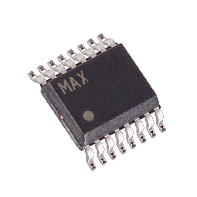
- Part No.:
- MAX964EEE+T
- Manufacturer:
- Analog Devices Inc./Maxim Integrated
- Category:
- Comparators
- Package:
- 16-SSOP (0.154", 3.90mm Width)
- Datasheet:
-
 MAX964EEE+T.pdf
- Description:
- IC COMPARATOR 4 GEN PUR 16QSOP
- Quantity:
- Payment:

- Shipping:

Inventory:2,075
Please send an inquiry. Send us your inquiry, and we will respond immediately.
Product details
Overview
MAX964EEE+T from Maxim Integrated is a quad ultra-high-speed comparator with internal hysteresis, optimized for single +3V or +5V operation. It features 4.5ns propagation delay (5mV overdrive), ±3.5mV input-referred hysteresis, rail-to-rail beyond-the-rails input range (–0.1V to VCC + 0.1V), and shutdown mode consuming only 270μA per comparator. It is used in high-speed sampling circuits and GPS receivers where precise, low-latency threshold detection is required.
For engineers reviewing the MAX964EEE+T datasheet, MAX964EEE+T pinout, MAX964EEE+T application, or MAX964EEE+T equivalent, key selection criteria include quad-channel count, 16-pin QSOP package, shutdown capability, TTL/CMOS-compatible outputs, and guaranteed 4.5ns propagation delay at 5mV overdrive under –40°C to +85°C operation.
Technical Context
The MAX964EEE+T implements a current-driven output stage enabling fast slew rates while maintaining VOH ≤ VCC – 0.52V and VOL ≥ 0.52V at 4mA load. Its internal 3.5mV hysteresis eliminates external feedback resistors and prevents oscillation near trip points.
It supports shutdown via SHDN pin (active-high), reducing supply current to 270μA per comparator and placing outputs in high-impedance state. Unlike MAX961/MAX963, it lacks latch-enable functionality but retains complementary output capability per channel - though MAX964 specifically provides non-complementary outputs as confirmed in the Selector Guide.
Key Specifications
| Parameter | Value and Actual Design Meaning |
|---|---|
| Propagation Delay | 4.5ns typical at 5mV overdrive - enables sub-5ns decision latency in timing-critical sampling paths |
| Supply Voltage Range | +2.7V to +5.5V - supports both 3V and 5V single-supply systems without level-shifting |
| Input Common-Mode Range | –0.1V to VCC + 0.1V - allows direct sensing of signals beyond supply rails, e.g., battery voltage monitoring |
| Output Drive Capability | Sinks/sources 4mA to within 0.52V of GND or VCC - drives standard TTL/CMOS loads without external pull-ups |
| Shutdown Current | 270μA per comparator - reduces total system quiescent power by >95% during idle periods |
| Hysteresis | 3.5mV input-referred - suppresses noise-induced chatter without requiring external resistor networks |
| Operating Temperature | –40°C to +85°C - qualified for industrial and portable equipment environments |
Pinout & Package
MAX964EEE+T is housed in a 16-pin QSOP (Quad Small Outline Package) with 0.15mm lead pitch and RoHS-compliant lead-free finish ("+" suffix). The package measures 4.9mm × 3.9mm × 1.45mm and is compatible with standard surface-mount reflow processes.
| Pin | Circuit Role | Design Meaning |
|---|---|---|
| 1 | INA− | Inverting input for Comparator A - accepts signals down to –0.1V relative to GND |
| 2 | N.C. | No connection - internally unconnected; tie to GND to prevent parasitic coupling |
| 3 | INA+ | Noninverting input for Comparator A - supports common-mode voltages up to VCC + 0.1V |
| 4 | QB | Output for Comparator B - TTL/CMOS-compatible, active-high, high-impedance in shutdown |
| 5 | VCC | Positive supply input - must be ≤ +5.5V; decoupling capacitor required adjacent to pin |
| 6 | GND | Ground reference - low-inductance plane connection critical for high-speed stability |
| 7 | QC | Output for Comparator C - matches QB electrical characteristics and timing behavior |
| 8 | QD | Output for Comparator D - identical drive strength and propagation delay to QA/QB/QC |
| 9 | SHDN | Active-high shutdown control - pulls high to enter low-power mode; requires clean logic transition |
| 10 | INC− | Inverting input for Comparator C - electrically isolated from other inputs; shares same hysteresis profile |
| 11 | INC+ | Noninverting input for Comparator C - differential pair matched to INA+/INA− for consistent offset |
| 12 | IND− | Inverting input for Comparator D - independent input path with same ESD protection structure |
| 13 | IND+ | Noninverting input for Comparator D - maintains <0.3ns inter-channel skew across all four comparators |
| 14 | INB− | Inverting input for Comparator B - referenced to same internal bias network as other channels |
| 15 | INB+ | Noninverting input for Comparator B - supports simultaneous multi-threshold detection with minimal crosstalk |
| 16 | QA | Output for Comparator A - primary output; synchronized with QB/QC/QD within 0.3ns skew |
Key Features
| Feature | Design Value |
|---|---|
| Ultra-fast 4.5ns propagation delay | Enables real-time signal edge detection in GPS baseband and high-speed data acquisition |
| Beyond-the-Rails™ input range | Accepts inputs 100mV below GND or above VCC - eliminates need for level-shifting in battery-monitoring circuits |
| Integrated 3.5mV hysteresis | Removes external resistor networks and associated board space, layout sensitivity, and temperature drift |
| Shutdown mode (270μA/comparator) | Reduces total quiescent current to <1.1mA for quad configuration - extends battery life in portable systems |
| TTL/CMOS-compatible outputs | Directly interfaces to FPGA I/O banks and microcontroller GPIO without external buffers or level translators |
| 16-pin QSOP package | Provides compact footprint (4.9 × 3.9 mm) with sufficient pin separation for high-speed routing and thermal relief |
Applications
| GPS Receiver Front-End | High-Speed Data Acquisition |
|---|---|
Use Scenario: Detecting zero-crossings and timing edges in L1-band IF signals after quadrature downconversion. IC Role / Device Role / Timing Role: Quad comparator simultaneously monitors I/Q channel thresholds to generate synchronous clock recovery pulses and symbol timing markers. Use Value: 4.5ns propagation delay ensures sub-10ns timing uncertainty in pulse generation, directly improving bit-error-rate performance in weak-signal conditions. |
Use Scenario: Converting analog sensor outputs (e.g., photodiode arrays, RF envelope detectors) into digital event triggers for time-of-flight or peak-detection systems. IC Role / Device Role / Timing Role: Four independent comparators implement parallel threshold windows for multi-level amplitude discrimination. Use Value: Matched propagation delay (<0.3ns skew) across all channels guarantees deterministic timing alignment between parallel decision paths. |
| Portable Battery Monitor | Industrial Line Receiver |
Use Scenario: Monitoring cell voltage, charge/discharge current sense, and thermal cutoff thresholds in handheld medical or test equipment. IC Role / Device Role / Timing Role: Simultaneous voltage window detection on multiple battery cells using shared VCC/GND with independent IN+/IN− pairs. Use Value: Beyond-the-Rails input range allows direct measurement of voltages slightly below GND (e.g., shunt-based current sensing) without op-amp front-end. |
Use Scenario: Receiving differential RS-422/RS-485-like signals in factory automation controllers where EMI immunity and fast response are critical. IC Role / Device Role / Timing Role: High-speed comparator converts noisy line signals into clean logic levels before FPGA-based protocol decoding. Use Value: 3.5mV internal hysteresis rejects broadband noise without degrading rise/fall time - maintains 2.3ns edge fidelity even with 50mVpp interference. |
Equivalent & Alternatives
The following parts are listed as comparable options for similar quad high-speed comparator applications.
| Alternative Part | Technical Difference | Application Difference | Selection Advice |
|---|---|---|---|
| LM339AQDRQ1 | Slower (1.3µs propagation delay), no internal hysteresis, no shutdown, wider supply range (2V–36V) | Automotive-qualified; suited for low-speed, high-voltage industrial monitoring - not viable for GPS or sampling circuits | Select only when speed <100ns is acceptable and rail-to-rail input is unnecessary |
| ADCMP572BCPZ-REEL7 | Faster (2.5ns), ECL/PECL outputs, no internal hysteresis, no shutdown, requires dual supplies (–5.2V/+5.2V) | Targeted at RF test equipment and optical receiver modules - incompatible with single 3V/5V logic domains | Choose only for ultra-low-jitter applications with dedicated ECL infrastructure and no power-constrained operation |
Compared with LM339AQDRQ1 and ADCMP572BCPZ-REEL7, MAX964EEE+T uniquely balances nanosecond-speed decision latency, single-supply operation, integrated hysteresis, and low-power shutdown - making it the only option suitable for portable, battery-powered, high-sample-rate systems requiring deterministic timing and minimal external components.
Availability
MAX964EEE+T is available at Aetrix Electronics and suitable for GPS receivers, high-speed data acquisition systems, and portable battery-monitoring applications requiring stable component supply, long-term lifecycle support, and RoHS-compliant packaging.
Supply support for MAX964EEE+T includes scheduled delivery planning, volume procurement assistance, BOM continuity management, traceable sourcing, and lifecycle availability coordination for OEM customers, industrial embedded developers, connected-device designers, and electronics production programs.
Manufacturer
Maxim Integrated (now part of Analog Devices) designs precision analog and mixed-signal ICs for industrial, communications, and consumer applications, with emphasis on integration, power efficiency, and reliability.
The MAX961–MAX964 family was developed to deliver ultra-high-speed comparator performance in single-supply, low-power portable systems - specifically targeting GPS, instrumentation, and real-time signal conditioning where latency, noise immunity, and board space are critical constraints.
FAQ
What is the operating temperature range for MAX964EEE+T?
The MAX964EEE+T is specified for operation from –40°C to +85°C, meeting industrial-grade environmental requirements. This range is explicitly confirmed in the Absolute Maximum Ratings and Electrical Characteristics tables for all E-grade devices including MAX964EEE+T. The "E" suffix denotes this extended temperature qualification, and the "+" indicates RoHS-compliant packaging.
Does MAX964EEE+T support latch-enable functionality like MAX961 or MAX963?
No, MAX964EEE+T does not include latch-enable functionality. Per the Selector Guide and Pin Description table, latch-enable (LE) is only present on MAX961 and MAX963. MAX964EEE+T has no LE pin and no internal latch circuitry - its outputs respond immediately to input transitions without storage capability. This is a deliberate functional distinction within the family.
What package type and dimensions does MAX964EEE+T use?
MAX964EEE+T uses a 16-pin QSOP (Quad Small Outline Package) with package code E16-1. Its dimensions are 4.9mm × 3.9mm × 1.45mm, and it features a 0.635mm lead pitch. The "+" suffix confirms it is lead(Pb)-free and RoHS-compliant, and land pattern number 90-0167 applies for PCB layout.
Can MAX964EEE+T operate from a 3.3V supply?
Yes, MAX964EEE+T fully supports 3.3V operation. Its supply voltage range is +2.7V to +5.5V, and all key specifications - including 4.5ns propagation delay, 3.5mV hysteresis, and output drive strength - are guaranteed across this range. Electrical Characteristics tables explicitly list data at VCC = 3.0V and 5.0V, confirming robust 3.3V compatibility.
How does the shutdown mode affect output states on MAX964EEE+T?
When SHDN is driven high, MAX964EEE+T enters shutdown mode: supply current drops to 270μA per comparator, and all four outputs (QA–QD) enter high-impedance state. Outputs remain floating - no pull-up or pull-down is activated internally. To ensure defined logic levels during shutdown, external termination resistors must be added at the system level if required.
MAX964EEE+T Specifications
- Product attributes
- Attribute value
- Manufacturer:
- Analog Devices Inc./Maxim Integrated
- Package/Case:
- 16-SSOP (0.154", 3.90mm Width)
- Series:
- Beyond-the-Rails™
- Packaging:
- Tape & Reel (TR)
- Product Status:
- Active
- Type:
- General Purpose
- Number of Elements:
- 4
- Output Type:
- CMOS, TTL
- Voltage - Supply, Single/Dual (±):
- 2.7V ~ 5.5V
- :
- 1.5mV @ 5V
- Voltage - Input Offset (Max):
- 15µA @ 5V
- Current - Input Bias (Max):
- -
- Current - Output (Typ):
- 9mA
- Current - Quiescent (Max):
- 80dB CMRR, 86.02dB PSRR
- CMRR, PSRR (Typ):
- 7ns
- Propagation Delay (Max):
- 3.5mV
- Hysteresis:
- -40°C ~ 85°C
- Operating Temperature:
- -
- Grade:
- -
- Qualification:
- Surface Mount
- :
- 16-QSOP
MAX964EEE+T FAQ
1.How can I place an order for MAX964EEE+T through Aetrix?
Please submit a Request for Quotation (RFQ) for MAX964EEE+T on Aetrix. Our sales agent will provide a competitive quotation and guide you through the order confirmation once you accept the terms.
2.Are the price and stock information for MAX964EEE+T reliable?
The price and inventory of MAX964EEE+T are updated periodically and may fluctuate due to market conditions. Stock and pricing data are typically refreshed every 24 hours. Quotation validity for MAX964EEE+T is usually 5 days.
3.What payment methods are accepted for MAX964EEE+T?
We accept Wire Transfer, PayPal, Credit Card, Western Union, MoneyGram, and Escrow for MAX964EEE+T transactions.
Note: Certain payment methods may incur a processing fee.
4.How is shipping managed for MAX964EEE+T?
MAX964EEE+T orders can be shipped via leading logistics carriers, including DHL, UPS, FedEx, TNT, or Registered Mail.
Once your MAX964EEE+T order is processed, you will receive an email with the shipment details and tracking number.
Note: Tracking information may take up to 24 hours to appear. Express delivery typically takes 3–5 business days.
5.How can I obtain technical support or documentation for MAX964EEE+T?
For technical support, including MAX964EEE+T datasheets, pinout diagrams, or application guidance, please contact our engineering support team. They can provide detailed documentation and assistance for your MAX964EEE+T requirements.
6.How does Aetrix verify that MAX964EEE+T is sourced from the original manufacturer or authorized distributors?
All MAX964EEE+T products on Aetrix are procured from qualified distributors and authorized channels. Our dedicated quality assurance team conducts strict verification, including traceability checks and, if necessary, third-party testing. This ensures that MAX964EEE+T meets industry standards.
7.What is the process for return or replacement of MAX964EEE+T?
All MAX964EEE+T units undergo pre-shipment inspection (PSI). If there is an issue with MAX964EEE+T, returns or replacements are accepted under the following conditions:
1.Quantity discrepancies, incorrect items, or visible external defects (such as breakage or corrosion), acknowledged by Aetrix.
2.The issue is reported within 90 days of delivery.
3.The MAX964EEE+T part is unused and in its original packaging.
Return procedure for MAX964EEE+T:
1.Submit a request within 90 days.
2.Obtain a Return Material Authorization (RMA) from Aetrix.
MAX964EEE+T Tags

-
LM2903DR
Texas Instruments

-
LM339DR
Texas Instruments

-
LM339PWR
Texas Instruments

-
LM393DT
STMicroelectronics
-
LM2901PWR
Texas Instruments
-
LM2903DT
STMicroelectronics
-
LM393DR
Texas Instruments
-
LM239DR
Texas Instruments
-
LM339APWR
Texas Instruments

-
LM2903P
Texas Instruments
-
LM393ADR
Texas Instruments
-
NCX2200GMAZ
NXP USA Inc.
Tech Hub

An engineering guide to LED driver operation, constant-current and constant-voltage outputs, linear and switching topologies, dimming, IC selection, calculations, replacement compatibility, and fault c…

Operational amplifier guide covering op amp basics, feedback, ideal vs real op amps, common configurations, buffer circuits, offset, bias current, gain-bandwidth, slew rate, rail-to-rail limits and sel…

Jumper cables guide covering safe connection order, red and black clamp placement, final ground connection, cable gauge, length, clamp quality, copper vs CCA cables, jump starter comparison and battery…

LDO regulator guide covering low dropout voltage, power dissipation, thermal design, PSRR, output noise, capacitor stability, adjustable LDO circuits, LDO vs buck converter and datasheet selection chec…

Conditional Access Module guide covering CAM meaning, CI/CI+ interface, smart card authorization, DVB security workflow, TV and set-top box compatibility, internal electronics, ESD protection, connecto…

Guide to electronic component obsolescence covering EOL risk, PCN/PDN notices, last-time buy planning, replacement options, form-fit-function validation, counterfeit risk and BOM lifecycle management.

18650 battery guide covering lithium-ion cell basics, 3.6V/3.7V voltage, 4.2V charging, mAh and Wh capacity, protected cells, chargers, BMS, series-parallel packs, holders, welding and sourcing checks.…

Hall effect sensor guide covering working principle, linear and digital sensors, Arduino circuits, current sensing, speed detection, automotive applications, A3144 examples, signal filtering and datash…

Product Change Notification guide for electronic components, covering PCN meaning, PCN vs PDN/EOL, common change types, risk levels, form-fit-function review, engineering validation, BOM control, LTB/L…

A practical guide to blend door actuators, covering HVAC function, symptoms, location, AC and heater issues, reset and calibration, replacement cost, electrical diagnosis, compatibility checks, and rep…


