
 My Inquiry
 My Account


Analog Devices Inc./Maxim Integrated MAX9667ETP+T
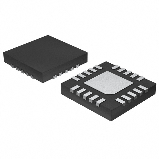
- Part No.:
- MAX9667ETP+T
- Manufacturer:
- Analog Devices Inc./Maxim Integrated
- Category:
- Video Processing
- Package:
- 20-WQFN Exposed Pad
- Datasheet:
-
 MAX9667ETP+T.pdf
- Description:
- IC VIDEO GAMMA REF SYST 20TQFN
- Quantity:
- Payment:

- Shipping:

Inventory:2,100
Please send an inquiry. Send us your inquiry, and we will respond immediately.
Product details
Overview
The MAX9667ETP+T from Maxim Integrated is a 10-channel, 10-bit nonvolatile programmable gamma and VCOM reference voltage generator for TFT LCD panels. It integrates ten gamma DAC buffers (six 10mA, four 5mA), one VCOM operational amplifier with 400mA peak sink/source capability, on-chip multiple-time programmable (MTP) memory (300 write cycles), I²C and single-wire interfaces, and supports AVDD up to 20V. It replaces discrete resistor strings, DVRs, and external VCOM amplifiers in high-resolution display timing systems.
For engineers reviewing the MAX9667ETP+T datasheet, MAX9667ETP+T pinout, MAX9667ETP+T application, or MAX9667ETP+T equivalent, key selection criteria include gamma channel count (10), VCOM transient current (±400mA), MTP endurance (300 writes), I²C timing compliance (400kHz), and thermal shutdown behavior (160°C).
Technical Context
The MAX9667ETP+T implements ten independent 10-bit DACs feeding gamma output buffers-six rated for 10mA DC/400mA transient, four for 5mA DC/200mA transient-and one dedicated VCOM op-amp with unity-gain stability into capacitive loads. All DACs share a common REF input (0–AVDD), enabling precise full-scale scaling per panel design.
It features dual digital control: an I²C interface (400kHz, standard-mode) for full register and MTP memory access, and a legacy-compatible single-wire CTL/CE interface for flicker-adjustment-only VCOM toggling. MTP memory auto-loads at power-up, and thermal protection disables non-central gamma outputs above 160°C while preserving VCOM functionality.
Key Specifications
| Parameter | Value and Actual Design Meaning |
|---|---|
| Gamma Channels | 10 independent outputs (OUT0–OUT9); enables full 10-point gamma correction for high-fidelity TFT-LCD grayscale rendering. |
| DAC Resolution | 10-bit (0–1023 code range); provides 0.1% full-scale step resolution for fine-grained voltage tuning. |
| VCOM Peak Current | ±400mA transient sink/source; sustains rapid backplane charging/discharging during polarity reversal without droop. |
| MTP Endurance | 300 write cycles; supports factory calibration and panel-specific gamma/VCOM optimization across production batches. |
| I²C Speed | 400kHz standard-mode; allows fast register updates during panel initialization or dynamic gamma adjustment. |
| Thermal Shutdown | 160°C junction temperature; disables non-central gamma outputs (OUT4/OUT5 remain active) to prevent thermal runaway while maintaining basic display function. |
| Supply Range (AVDD) | 9V to 20V; accommodates high-voltage TFT bias rails without external regulators or level-shifting circuitry. |
Pinout & Package
MAX9667ETP+T uses a 20-pin TQFN-EP package (5mm × 5mm, exposed pad). The exposed pad must be connected to digital ground for thermal and electrical integrity.
| Pin/Terminal | Circuit Role | Design Meaning |
|---|---|---|
| 1 CE | Single-wire interface enable | Active-high control: DVDD enables CTL pulse decoding for VCOM flicker adjustment; GND disables CTL and reduces quiescent current. |
| 2 DVDD | Digital supply input | 2.7–3.6V logic rail; requires 0.1µF bypass to GND for stable I²C and MTP programming operation. |
| 3 SCL | I²C clock input | Drives synchronous serial communication; supports 400kHz max frequency with 1.3µs low-pulse width minimum. |
| 4 SDA | I²C data I/O | Open-drain bidirectional line; requires pull-up to DVDD; handles full register read/write and MTP command execution. |
| 5 GND | Ground reference | Common return for analog/digital domains; exposed pad must connect here for thermal dissipation and noise control. |
| 6–15 OUT9–OUT0 | Gamma DAC buffered outputs | 10 dedicated channels: OUT0/OUT4/OUT5/OUT9 = 10mA buffers; OUT1/OUT2/OUT3/OUT6/OUT7/OUT8 = 5mA buffers. |
| 16 REF | DAC reference input | Analog voltage source (0–AVDD) setting full-scale DAC output; determines gamma voltage range and linearity. |
| 17 AVDD | Analog supply input | 9–20V high-voltage rail; powers all DACs and VCOM amplifier; requires ≥0.1µF ceramic bypass to GND. |
| 18 FB | VCOM amplifier inverting input | Connects directly to VCOM pin for unity-gain configuration; supports external feedback resistors for gain >1. |
| 19 VCOM | VCOM amplifier output | High-current (±400mA) driver for LCD backplane; capable of direct capacitive load driving without series resistance. |
| 20 CTL | VCOM/MTP control input | Pulse-driven interface: short pulses adjust VCOM up/down; specific voltage ramp/timing required for MTP programming. |
Key Features
| Feature | Design Value |
|---|---|
| Integrated MTP memory | Stores gamma and VCOM DAC codes nonvolatily across 300 write cycles-eliminates external EEPROM and enables panel-specific calibration persistence. |
| 10mA/5mA gamma buffer split | Optimizes drive strength: 10mA buffers drive resistor ladder ends (high-current nodes); 5mA buffers serve midpoints-reducing power and layout complexity. |
| VCOM op-amp with current limiting | Provides ±400mA transient current into LCD backplane while protecting bond wires from overcurrent damage during polarity switching. |
| 40dB horizontal noise suppression | Internal DAC lowpass filtering attenuates 60kHz line-frequency noise from AVDD-reducing visible flicker without external RC networks. |
| Thermal-aware gamma disable | At 160°C, only central gamma outputs (OUT4/OUT5) remain active-preserving partial display functionality during thermal stress events. |
Applications
| High-Resolution TFT-LCD Panels | Automotive Instrument Clusters |
|---|---|
Use Scenario: Driving 10-point gamma correction and dynamic VCOM adjustment in 4K UHD LCD modules with tight grayscale uniformity requirements. IC Role / Device Role / Timing Role: Central gamma/VCOM reference generator; replaces discrete resistor ladders, DVRs, and external op-amps in the display timing chain. Use Value: Enables factory-per-panel gamma calibration via MTP memory, reducing yield loss and eliminating manual resistor trimming. | Use Scenario: Providing stable, flicker-free backlight and segment voltage references in automotive-grade digital instrument clusters operating from -40°C to +85°C. IC Role / Device Role / Timing Role: High-reliability analog reference IC with thermal shutdown and wide AVDD range (9–20V) compatible with automotive battery transients. Use Value: Single-chip solution eliminates 7+ discrete components, improving BOM simplicity and long-term calibration retention under thermal cycling. |
| Industrial HMI Displays | Medical Imaging Monitors |
Use Scenario: Supporting gamma consistency across multi-year production runs of industrial touchscreens exposed to variable ambient temperatures. IC Role / Device Role / Timing Role: Nonvolatile programmable reference IC with 300-cycle MTP endurance and ±0.5mV/mA load regulation for stable grayscale tracking. Use Value: Maintains calibrated gamma curves over product lifetime without recalibration-critical for consistent UI appearance in factory environments. | Use Scenario: Delivering precise, low-noise gamma voltages and flicker-minimized VCOM for diagnostic-grade grayscale accuracy in DICOM-compliant medical monitors. IC Role / Device Role / Timing Role: High-PSRR (≥70dB) gamma/VCOM reference IC with <±40mV total output error at code 512-meeting clinical display fidelity standards. Use Value: Reduces image banding and luminance drift through superior power-supply rejection and thermal stability across operating conditions. |
Equivalent & Alternatives
The following parts are listed as comparable options for similar gamma and VCOM reference applications.
| Alternative Part | Technical Difference | Application Difference | Selection Advice |
|---|---|---|---|
| MAX9666ETP+T | 8 gamma channels, same 10-bit DAC resolution, identical MTP endurance (300 cycles), I²C/single-wire interfaces, and VCOM architecture. | Suitable for mid-resolution panels requiring fewer gamma points; occupies same 20-pin TQFN footprint but drives only 8 gamma nodes. | Select when panel design uses ≤8 gamma taps-reduces cost and simplifies firmware without sacrificing VCOM performance or calibration depth. |
| MAX9665ETP+T | 6 gamma channels, otherwise identical architecture, pinout, and electrical specs-including VCOM op-amp, MTP, and interface compatibility. | Targeted at entry-level or legacy TFT designs with simpler gamma curves; shares identical thermal shutdown and PSRR behavior. | Choose for cost-sensitive or space-constrained applications where 6-point gamma suffices-enables drop-in PCB reuse with minimal firmware changes. |
Compared with MAX9666ETP+T and MAX9665ETP+T, the MAX9667ETP+T delivers two additional gamma channels (10 vs. 8 or 6) while retaining identical VCOM drive strength, MTP reliability, and thermal protection-making it the optimal choice for next-generation high-fidelity displays demanding full 10-point correction.
Availability
MAX9667ETP+T is available at Aetrix Electronics and suitable for high-resolution TFT-LCD panels, automotive instrument clusters, and medical imaging monitors requiring stable component supply, long-term calibration retention, and robust thermal management.
Supply support for MAX9667ETP+T includes scheduled delivery planning, volume procurement assistance, BOM continuity management, traceable sourcing, and lifecycle availability coordination for OEM customers, industrial embedded developers, connected-device designers, and electronics production programs.
Manufacturer
Maxim Integrated (now part of Analog Devices) designs precision analog and mixed-signal ICs for power, sensing, interface, and timing applications in industrial, automotive, and consumer systems.
The MAX9667ETP+T belongs to Maxim's TFT-LCD gamma/VCOM reference family, engineered specifically to replace discrete resistor strings and external amplifiers with a single-chip, nonvolatile, high-current solution for display calibration and stability.
FAQ
What is the maximum number of gamma channels supported by the MAX9667ETP+T?
The MAX9667ETP+T supports exactly 10 gamma channels (OUT0 through OUT9), as confirmed in the Ordering Information table and Functional Diagram. This distinguishes it from the 6-channel MAX9665ETP+T and 8-channel MAX9666ETP+T variants within the same family. Each channel features a dedicated 10-bit DAC and buffer optimized for TFT-LCD gamma correction.
Does the MAX9667ETP+T include nonvolatile memory, and how many write cycles does it support?
Yes, the MAX9667ETP+T integrates on-chip multiple-time programmable (MTP) memory that retains gamma and VCOM DAC codes without power. Per the datasheet Absolute Maximum Ratings and Detailed Description sections, this MTP memory supports up to 300 write operations-sufficient for factory calibration and panel-specific tuning across production lifecycles.
What is the peak output current capability of the VCOM amplifier in the MAX9667ETP+T?
The VCOM amplifier in the MAX9667ETP+T delivers ±400mA peak transient current, as specified in the Electrical Characteristics table under "VCOM OUTPUT" and confirmed in the Detailed Description section. This enables robust driving of large-area TFT-LCD backplanes during polarity switching without output droop or recovery delay.
Can the MAX9667ETP+T be used with both I²C and single-wire interfaces simultaneously?
No-the MAX9667ETP+T enforces strict interface arbitration: operation through one interface is blocked while the other is active. As stated in the Interoperability section, if the I²C interface is executing a command, inputs on the single-wire interface (CTL/CE) are ignored, and vice versa. This prevents register corruption during concurrent access.
What package type and thermal characteristics apply to the MAX9667ETP+T?
The MAX9667ETP+T uses a 20-pin TQFN-EP package (5mm × 5mm) with an exposed pad that must be soldered to a digital ground plane. Its thermal characteristics include θJA = 39°C/W and θJC = 6°C/W (per JEDEC JESD51-7), and it activates thermal shutdown at 160°C junction temperature-disabling non-central gamma outputs while preserving VCOM and OUT4/OUT5 functionality.
MAX9667ETP+T Specifications
- Product attributes
- Attribute value
- Manufacturer:
- Analog Devices Inc./Maxim Integrated
- Series:
- -
- Package/Case:
- 20-WQFN Exposed Pad
- Packaging:
- Tape & Reel (TR)
- Product Status:
- Obsolete
- Function:
- Gamma Reference
- Applications:
- Video Display
- Standards:
- -
- Control Interface:
- I2C, Serial
- Voltage - Supply:
- 2.7V ~ 3.6V
- Mounting Type:
- Surface Mount
- Grade:
- -
- Qualification:
- -
- Supplier Device Package:
- 20-TQFN (5x5)
MAX9667ETP+T FAQ
1.How can I place an order for MAX9667ETP+T through Aetrix?
Please submit a Request for Quotation (RFQ) for MAX9667ETP+T on Aetrix. Our sales agent will provide a competitive quotation and guide you through the order confirmation once you accept the terms.
2.Are the price and stock information for MAX9667ETP+T reliable?
The price and inventory of MAX9667ETP+T are updated periodically and may fluctuate due to market conditions. Stock and pricing data are typically refreshed every 24 hours. Quotation validity for MAX9667ETP+T is usually 5 days.
3.What payment methods are accepted for MAX9667ETP+T?
We accept Wire Transfer, PayPal, Credit Card, Western Union, MoneyGram, and Escrow for MAX9667ETP+T transactions.
Note: Certain payment methods may incur a processing fee.
4.How is shipping managed for MAX9667ETP+T?
MAX9667ETP+T orders can be shipped via leading logistics carriers, including DHL, UPS, FedEx, TNT, or Registered Mail.
Once your MAX9667ETP+T order is processed, you will receive an email with the shipment details and tracking number.
Note: Tracking information may take up to 24 hours to appear. Express delivery typically takes 3–5 business days.
5.How can I obtain technical support or documentation for MAX9667ETP+T?
For technical support, including MAX9667ETP+T datasheets, pinout diagrams, or application guidance, please contact our engineering support team. They can provide detailed documentation and assistance for your MAX9667ETP+T requirements.
6.How does Aetrix verify that MAX9667ETP+T is sourced from the original manufacturer or authorized distributors?
All MAX9667ETP+T products on Aetrix are procured from qualified distributors and authorized channels. Our dedicated quality assurance team conducts strict verification, including traceability checks and, if necessary, third-party testing. This ensures that MAX9667ETP+T meets industry standards.
7.What is the process for return or replacement of MAX9667ETP+T?
All MAX9667ETP+T units undergo pre-shipment inspection (PSI). If there is an issue with MAX9667ETP+T, returns or replacements are accepted under the following conditions:
1.Quantity discrepancies, incorrect items, or visible external defects (such as breakage or corrosion), acknowledged by Aetrix.
2.The issue is reported within 90 days of delivery.
3.The MAX9667ETP+T part is unused and in its original packaging.
Return procedure for MAX9667ETP+T:
1.Submit a request within 90 days.
2.Obtain a Return Material Authorization (RMA) from Aetrix.
MAX9667ETP+T Tags

-
HDMI2C1-6C1
STMicroelectronics

-
ADA4430-1YKSZ-R7
Analog Devices Inc.

-
LM1881MX/NOPB
Texas Instruments

-
SN75DP130SSRGZR
Texas Instruments

-
EQCO30T5.2
Microchip Technology

-
LMH1980MM/NOPB
Texas Instruments
-
EQCO30R5.D
Microchip Technology

-
SII9022ACNU
Lattice Semiconductor Corporation
-
SN65DP159RGZR
Texas Instruments

-
SN65DP159RSBR
Texas Instruments

-
SN65DP141RLJR
Texas Instruments

-
LMH0303SQ/NOPB
Texas Instruments
Tech Hub

A practical engineering guide to 3.3V and 5V logic compatibility, input thresholds, resistor dividers, translator ICs, MOSFET level shifting, I2C pull-ups, timing limits and power-sequencing risks.

The 74HC595 uses push-pull logic outputs, while the TPIC6B595 uses 50 V open-drain DMOS sinks for higher-power loads. This guide compares timing, current limits, 3.3 V interfacing, load wiring, thermal…

The 74HC595 converts serial data into eight stable parallel outputs. This guide covers pin functions, shift and storage timing, OE and MR behavior, drive-current limits, cascading, voltage compatibilit…

A technical comparison of level-sensitive latches and edge-triggered flip-flops, covering timing windows, setup and hold limits, master–slave operation, time borrowing, race-through, HDL inference and…

A D latch stores one bit while Enable controls when data can pass. This reference covers gate-level operation, truth tables, transparency, setup and hold timing, LE versus OE, common ICs and practical …

An SR latch stores one bit through cross-coupled feedback. This engineering reference covers NOR and NAND implementations, truth tables, forbidden-state recovery, gated operation, switch debouncing, fa…

Latch circuits retain one bit through feedback. This technical reference covers SR and D latches, truth tables, transparency, timing limits, latch-versus-flip-flop behavior, applications and common log…

An engineering guide to LED driver operation, constant-current and constant-voltage outputs, linear and switching topologies, dimming, IC selection, calculations, replacement compatibility, and fault c…

Operational amplifier guide covering op amp basics, feedback, ideal vs real op amps, common configurations, buffer circuits, offset, bias current, gain-bandwidth, slew rate, rail-to-rail limits and sel…

Jumper cables guide covering safe connection order, red and black clamp placement, final ground connection, cable gauge, length, clamp quality, copper vs CCA cables, jump starter comparison and battery…


