
 My Inquiry
 My Account


Analog Devices Inc./Maxim Integrated MAX9669ETI+T
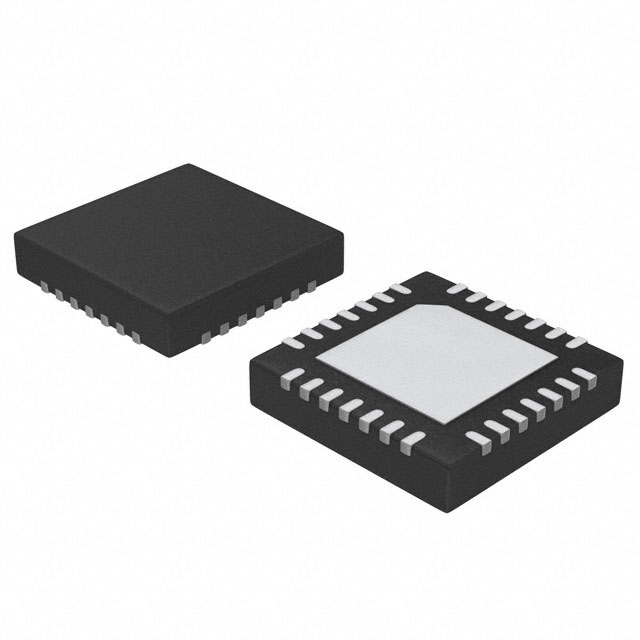
- Part No.:
- MAX9669ETI+T
- Manufacturer:
- Analog Devices Inc./Maxim Integrated
- Category:
- Video Processing
- Package:
- 28-WFQFN Exposed Pad
- Datasheet:
-
 MAX9669ETI+T.pdf
- Description:
- IC VIDEO GAMMA REF SYST 28TQFN
- Quantity:
- Payment:

- Shipping:

Inventory:4,854
Please send an inquiry. Send us your inquiry, and we will respond immediately.
Product details
Overview
MAX9669ETI+T from Maxim Integrated is a 10-bit programmable gamma reference IC with integrated MTP memory, designed specifically for TFT LCD panel gamma correction and VCOM voltage generation. It delivers 16 buffered gamma reference outputs (each with 10-bit DAC + buffer) and one amplified VCOM output (10-bit DAC + op-amp), supporting analog supplies from 9V to 20V and digital supply from 2.7V to 3.6V. Its 1µs settling time and 200mA/600mA peak transient drive capability enable stable voltage delivery during critical display patterns.
For engineers reviewing the MAX9669ETI+T datasheet, MAX9669ETI+T pinout, MAX9669ETI+T application, or MAX9669ETI+T equivalent, this page provides verified technical context, confirmed pin functions, real-world TFT LCD system integration details, and validated alternative options - all grounded in the official MAX9669 datasheet Rev 4 (8/11).
Technical Context
The MAX9669ETI+T integrates seventeen 10-bit DACs: sixteen gamma channels use rail-to-rail output buffers, while the VCOM channel uses a dedicated high-current amplifier with internal current limiting and thermal shutdown at +165°C. All DAC outputs are referenced to AVDD (9–20V), with output equations strictly defined as VOUT = (VAVDD × CODE)/1024.
Programming occurs via I²C interface (up to 400kHz) using a 7-bit slave address configurable by A0 pin, with separate volatile register and nonvolatile MTP memory banks. The MTP supports up to 100 write cycles and stores factory- or user-programmed gamma/VCOM values, eliminating external EEPROM in production-line automatic calibration workflows.
Key Specifications
| Parameter | Value and Actual Design Meaning |
|---|---|
| Gamma Channels | 16 independent 10-bit DACs with output buffers; each sources/sinks 10mA DC within 200mV of rails and handles 200mA peak transients. |
| VCOM Channel | 10-bit DAC with integrated op-amp; delivers 600mA peak transient current and settles in 1µs, enabling direct drive of large LCD backplane capacitance. |
| Analog Supply Range | 9V to 20V on AVDD and AVDD_AMP; supports high-voltage TFT biasing without external regulators. |
| Digital Supply Range | 2.7V to 3.6V on DVDD; compatible with standard 3.3V logic systems and low-power microcontrollers. |
| I²C Interface | Standard-mode (400kHz max); supports slave address selection via A0 pin and auto-incrementing register reads/writes for efficient bulk programming. |
| MTP Memory | On-chip multiple-time programmable nonvolatile memory; retains gamma/VCOM settings across power cycles and supports ≤100 writes for production calibration. |
| Settling Time | 1µs for both gamma and VCOM outputs; ensures minimal voltage glitch during rapid grayscale transitions in moving video content. |
Pinout & Package
MAX9669ETI+T is housed in a 28-pin Thin QFN with exposed pad (5mm × 5mm), RoHS-compliant and lead-free. The exposed pad (EP) is internally connected to DGND and must be soldered to the PCB's digital ground plane for thermal and electrical performance.
| Pin/Terminal | Circuit Role | Design Meaning |
|---|---|---|
| 1, 12–28 (GMA1–GMA16) | Gamma DAC analog outputs | 16 buffered voltage references for LCD column driver gamma correction; each capable of ±200mA peak current. |
| 2 (SCL) | I²C serial clock input | Master-generated clock line; requires pull-up resistor ≥500Ω if shared bus or open-drain master. |
| 3 (SDA) | I²C serial data I/O | Open-drain bidirectional data line; requires external pull-up resistor ≥500Ω and supports ACK/NACK handshaking. |
| 4 (A0) | I²C device address bit | Selects LSB of 7-bit slave address (E8h/E9h or EAh/EBh depending on A0 logic level). |
| 5 (DVDD) | Digital power supply | 3.3V nominal supply for logic core and I²C interface; bypass with 0.1µF capacitor to EP. |
| 6 (AGND_AMP) | VCOM amplifier ground | Separate analog ground for VCOM op-amp; improves PSRR and reduces crosstalk between gamma and VCOM paths. |
| 7 (VCOM) | VCOM amplifier output | High-current common voltage output for TFT LCD backplane; drives capacitive loads directly without series resistor. |
| 8 (VCOM_FB) | VCOM amplifier feedback | Connects to VCOM output for unity-gain configuration; enables precise closed-loop regulation. |
| 9 (AVDD_AMP) | VCOM amplifier analog supply | Independent 9–20V supply for VCOM op-amp; decoupled with 0.1µF capacitor to AGND_AMP. |
| 10, 20 (AVDD) | Gamma DAC analog supply | Main analog rail for gamma DACs; sets full-scale output range (VOUT = VAVDD × CODE / 1024). |
| 11, 21 (AGND) | Gamma DAC analog ground | Reference ground for gamma DACs and buffers; kept separate from digital ground to minimize noise coupling. |
| EP | Exposed thermal pad | Internally tied to DGND; mandatory connection to PCB digital ground plane for thermal dissipation and EMI control. |
Key Features
| Feature | Design Value |
|---|---|
| Integrated MTP memory | Eliminates external EEPROM; stores calibrated gamma/VCOM values on-chip for panel-by-panel factory calibration. |
| Programmable VCOM limits | VCOMMIN/VCOMMAX registers constrain VCOM DAC output to prevent overvoltage or undervoltage conditions during dynamic updates. |
| 1µs fast settling time | Enables accurate gamma voltage establishment before next horizontal line scan, reducing flicker and banding artifacts. |
| Channel-to-channel isolation | 80dB at 5MHz prevents crosstalk between adjacent gamma outputs, preserving grayscale fidelity across wide viewing angles. |
| Thermal shutdown protection | Disables gamma outputs at +165°C with 15°C hysteresis; protects bond wires and maintains reliability under sustained high-load conditions. |
Applications
| Gamma Calibration System | VCOM Voltage Generation |
|---|---|
|
Use Scenario: Automated gamma tuning during TFT LCD panel manufacturing, where each panel receives unique gamma curve compensation based on optical sensor feedback. IC Role / Device Role / Timing Role: Primary gamma reference generator; 16 DAC outputs feed column driver ICs to define grayscale voltage levels per pixel row. Use Value: Enables panel-level binning and compensation without external DACs or resistive strings, reducing BOM count and test time. |
Use Scenario: Maintaining stable common electrode voltage across large-format TFT displays during video playback with varying image content. IC Role / Device Role / Timing Role: High-current VCOM driver; regulates backplane voltage with <1µs response to counteract charge injection from source drivers. Use Value: Reduces flicker and image retention by delivering 600mA peak current directly to LCD capacitance, avoiding external op-amp stages. |
| Production-Line Flicker Correction | Integrated LCD Power Management |
|
Use Scenario: Real-time VCOM adjustment during final QA testing to suppress AC-coupled flicker caused by panel aging or temperature drift. IC Role / Device Role / Timing Role: Programmable VCOM reference with MTP storage; allows post-calibration lock-in of optimized VCOM value per panel lot. Use Value: Supports automatic flicker calibration via I²C commands, eliminating manual potentiometer tuning and improving yield consistency. |
Use Scenario: Consolidating discrete gamma buffers, VCOM amplifier, and high-voltage regulator into a single chip for compact LCD module designs. IC Role / Device Role / Timing Role: Centralized reference voltage subsystem; generates all panel bias voltages (gamma, VCOM, level-shift) from one IC. Use Value: Cuts PCB area by >40% versus discrete solution and simplifies power sequencing-no external HV LDO needed due to DAC lowpass filtering. |
Equivalent & Alternatives
The following parts are listed as comparable options for similar gamma reference and VCOM driver applications.
| Alternative Part | Technical Difference | Application Difference | Selection Advice |
|---|---|---|---|
| MAX9650ETJ+T | Dedicated VCOM power amplifier only (no gamma DACs); 1A sink/source capability; requires external DAC and reference. | Used when higher VCOM current (>600mA) is required, but gamma correction is handled separately. | Select MAX9650ETJ+T only if MAX9669ETI+T's 600mA VCOM drive is insufficient and system already includes gamma DACs. |
| DS3930S+ | 16-channel gamma DAC with EEPROM, but no integrated VCOM amplifier; 100mA gamma drive; 2.7–5.5V analog supply only. | Suitable for low-voltage portable LCDs (e.g., tablets), not high-voltage industrial panels requiring 9–20V operation. | Choose DS3930S+ only for cost-sensitive, low-power applications where VCOM is generated externally and AVDD < 6V. |
Compared with MAX9650ETJ+T and DS3930S+, the MAX9669ETI+T uniquely integrates both gamma correction and high-current VCOM drive in a single 9–20V analog supply domain, eliminating external components while supporting production-line programmability and thermal robustness for large TFT panels.
Availability
MAX9669ETI+T is available at Aetrix Electronics and suitable for TFT LCD manufacturing, display module design, and industrial HMI development requiring stable component supply, long-term lifecycle support, and guaranteed RoHS compliance.
Supply support for MAX9669ETI+T includes scheduled delivery planning, volume procurement assistance, BOM continuity management, traceable sourcing, and lifecycle availability coordination for OEM customers, industrial embedded developers, connected-device designers, and electronics production programs.
Manufacturer
Maxim Integrated (now part of Analog Devices) is a semiconductor company specializing in precision analog, mixed-signal, and power management ICs for industrial, automotive, and consumer applications.
The MAX9669ETI+T belongs to Maxim's display power and timing product line, engineered to consolidate gamma correction, VCOM generation, and programmable calibration into a single IC for high-reliability TFT LCD systems.
FAQ
What is the maximum analog supply voltage supported by the MAX9669ETI+T?
The MAX9669ETI+T supports an analog supply voltage range of 9V to 20V on both AVDD and AVDD_AMP pins. Absolute maximum rating is +22V, but operation above 20V voids specifications and risks permanent damage. For reliable long-term performance, AVDD and AVDD_AMP should be maintained within the 9–20V range specified in the MAX9669ETI+T datasheet.
Does the MAX9669ETI+T require external EEPROM for gamma calibration storage?
No, the MAX9669ETI+T does not require external EEPROM. It features integrated multiple-time programmable (MTP) memory that stores gamma and VCOM values on-chip. This MTP memory supports up to 100 write cycles and retains settings across power cycles, enabling panel-specific calibration without additional components.
How many I²C addresses does the MAX9669ETI+T support, and how are they selected?
The MAX9669ETI+T supports four I²C slave addresses: E8h, E9h, EAh, and EBh. Address selection is controlled by the logic level on the A0 pin and the DVDD supply state. When DVDD is present, A0 = low selects E8h/E9h; A0 = high selects EAh/EBh. The R/W bit determines read (1) or write (0) mode, yielding two addresses per A0 state.
What is the purpose of the VCOMMIN and VCOMMAX registers in the MAX9669ETI+T?
The VCOMMIN and VCOMMAX registers in the MAX9669ETI+T define software-enforced upper and lower bounds for the VCOM DAC output. If the VCOM register is written with a value outside this range, it automatically clamps to the nearest limit. This prevents accidental overvoltage or undervoltage conditions during dynamic updates, enhancing system safety and display stability.
Can the MAX9669ETI+T drive large LCD panels without external buffering?
Yes, the MAX9669ETI+T can drive large LCD panels directly via its VCOM amplifier, which delivers 600mA peak current and settles in 1µs. Its integrated op-amp is designed to drive typical TFT backplane capacitance without series resistors. However, for panels requiring >600mA, Maxim recommends buffering the VCOM output with the MAX9650ETJ+T amplifier.
MAX9669ETI+T Specifications
- Product attributes
- Attribute value
- Manufacturer:
- Analog Devices Inc./Maxim Integrated
- Series:
- -
- Package/Case:
- 28-WFQFN Exposed Pad
- Packaging:
- Tape & Reel (TR)
- Product Status:
- Obsolete
- Function:
- Gamma Reference
- Applications:
- Video Display
- Standards:
- -
- Control Interface:
- I2C
- Voltage - Supply:
- 2.7V ~ 3.6V
- Mounting Type:
- Surface Mount
- Grade:
- -
- Qualification:
- -
- Supplier Device Package:
- 28-TQFN (5x5)
MAX9669ETI+T FAQ
1.How can I place an order for MAX9669ETI+T through Aetrix?
Please submit a Request for Quotation (RFQ) for MAX9669ETI+T on Aetrix. Our sales agent will provide a competitive quotation and guide you through the order confirmation once you accept the terms.
2.Are the price and stock information for MAX9669ETI+T reliable?
The price and inventory of MAX9669ETI+T are updated periodically and may fluctuate due to market conditions. Stock and pricing data are typically refreshed every 24 hours. Quotation validity for MAX9669ETI+T is usually 5 days.
3.What payment methods are accepted for MAX9669ETI+T?
We accept Wire Transfer, PayPal, Credit Card, Western Union, MoneyGram, and Escrow for MAX9669ETI+T transactions.
Note: Certain payment methods may incur a processing fee.
4.How is shipping managed for MAX9669ETI+T?
MAX9669ETI+T orders can be shipped via leading logistics carriers, including DHL, UPS, FedEx, TNT, or Registered Mail.
Once your MAX9669ETI+T order is processed, you will receive an email with the shipment details and tracking number.
Note: Tracking information may take up to 24 hours to appear. Express delivery typically takes 3–5 business days.
5.How can I obtain technical support or documentation for MAX9669ETI+T?
For technical support, including MAX9669ETI+T datasheets, pinout diagrams, or application guidance, please contact our engineering support team. They can provide detailed documentation and assistance for your MAX9669ETI+T requirements.
6.How does Aetrix verify that MAX9669ETI+T is sourced from the original manufacturer or authorized distributors?
All MAX9669ETI+T products on Aetrix are procured from qualified distributors and authorized channels. Our dedicated quality assurance team conducts strict verification, including traceability checks and, if necessary, third-party testing. This ensures that MAX9669ETI+T meets industry standards.
7.What is the process for return or replacement of MAX9669ETI+T?
All MAX9669ETI+T units undergo pre-shipment inspection (PSI). If there is an issue with MAX9669ETI+T, returns or replacements are accepted under the following conditions:
1.Quantity discrepancies, incorrect items, or visible external defects (such as breakage or corrosion), acknowledged by Aetrix.
2.The issue is reported within 90 days of delivery.
3.The MAX9669ETI+T part is unused and in its original packaging.
Return procedure for MAX9669ETI+T:
1.Submit a request within 90 days.
2.Obtain a Return Material Authorization (RMA) from Aetrix.
MAX9669ETI+T Tags

-
HDMI2C1-6C1
STMicroelectronics

-
ADA4430-1YKSZ-R7
Analog Devices Inc.

-
LM1881MX/NOPB
Texas Instruments

-
SN75DP130SSRGZR
Texas Instruments

-
EQCO30T5.2
Microchip Technology

-
LMH1980MM/NOPB
Texas Instruments
-
EQCO30R5.D
Microchip Technology

-
SII9022ACNU
Lattice Semiconductor Corporation
-
SN65DP159RGZR
Texas Instruments

-
SN65DP159RSBR
Texas Instruments

-
SN65DP141RLJR
Texas Instruments

-
LMH0303SQ/NOPB
Texas Instruments
Tech Hub

A practical engineering guide to 3.3V and 5V logic compatibility, input thresholds, resistor dividers, translator ICs, MOSFET level shifting, I2C pull-ups, timing limits and power-sequencing risks.

The 74HC595 uses push-pull logic outputs, while the TPIC6B595 uses 50 V open-drain DMOS sinks for higher-power loads. This guide compares timing, current limits, 3.3 V interfacing, load wiring, thermal…

The 74HC595 converts serial data into eight stable parallel outputs. This guide covers pin functions, shift and storage timing, OE and MR behavior, drive-current limits, cascading, voltage compatibilit…

A technical comparison of level-sensitive latches and edge-triggered flip-flops, covering timing windows, setup and hold limits, master–slave operation, time borrowing, race-through, HDL inference and…

A D latch stores one bit while Enable controls when data can pass. This reference covers gate-level operation, truth tables, transparency, setup and hold timing, LE versus OE, common ICs and practical …

An SR latch stores one bit through cross-coupled feedback. This engineering reference covers NOR and NAND implementations, truth tables, forbidden-state recovery, gated operation, switch debouncing, fa…

Latch circuits retain one bit through feedback. This technical reference covers SR and D latches, truth tables, transparency, timing limits, latch-versus-flip-flop behavior, applications and common log…

An engineering guide to LED driver operation, constant-current and constant-voltage outputs, linear and switching topologies, dimming, IC selection, calculations, replacement compatibility, and fault c…

Operational amplifier guide covering op amp basics, feedback, ideal vs real op amps, common configurations, buffer circuits, offset, bias current, gain-bandwidth, slew rate, rail-to-rail limits and sel…

Jumper cables guide covering safe connection order, red and black clamp placement, final ground connection, cable gauge, length, clamp quality, copper vs CCA cables, jump starter comparison and battery…


