
 My Inquiry
 My Account


Analog Devices Inc./Maxim Integrated MAX9892ERT+T
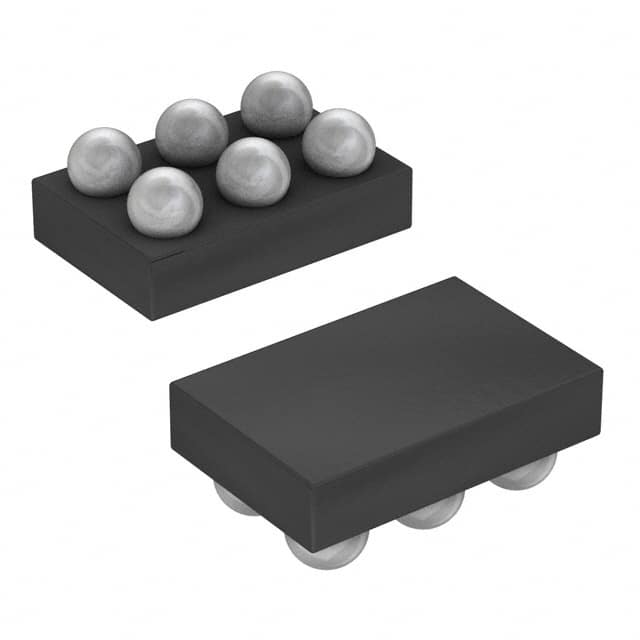
- Part No.:
- MAX9892ERT+T
- Manufacturer:
- Analog Devices Inc./Maxim Integrated
- Category:
- Audio Special Purpose
- Package:
- 6-WFBGA, CSPBGA
- Datasheet:
-
 MAX9892ERT+T.pdf
- Description:
- IC NOISE REDUCTION 6UCSP
- Quantity:
- Payment:

- Shipping:

Inventory:2,149
Please send an inquiry. Send us your inquiry, and we will respond immediately.
Product details
Overview
The MAX9892ERT+T from Maxim Integrated is a shunt-mode audio click-and-pop eliminator designed to suppress transient noise at amplifier startup/shutdown in portable headphone systems. It operates from 1.7V to 3.6V, features <1µA supply current, 0.3Ω typical switch on-resistance at 3.0V, adjustable turn-off delay (1ms–1000ms via external CSET), and interfaces directly with left/right amplifier outputs to ground during mute transitions. Used in smartphones and portable media players.
For engineers reviewing the MAX9892ERT+T datasheet, MAX9892ERT+T pinout, MAX9892ERT+T application, or MAX9892ERT+T equivalent, key selection criteria include guaranteed -40°C to +85°C operation, UCSP-6 package dimensions (1mm × 1.52mm × 0.6mm), input voltage tolerance down to VDD − 5.5V, 130ns turn-on time, and 35dB click-and-pop reduction with 30Ω series resistors.
Technical Context
The MAX9892ERT+T implements two independent low-impedance analog switches controlled by an active-low MUTE signal. During normal operation, switches remain open and introduce no signal path loading; during power transitions, they close to shunt amplifier output nodes to ground, preventing audible transients caused by DC-blocking capacitor discharge.
Turn-off timing is programmable via external capacitor (CSET) connected between SET and GND, enabling precise alignment with amplifier startup profiles. Input voltage range supports rail-to-rail audio swing relative to VDD (down to VDD − 5.5V), ensuring compatibility with common ±2V headphone signals when VDD is set between 2.0V and 3.5V.
Key Specifications
| Parameter | Value and Actual Design Meaning |
|---|---|
| Supply Voltage Range | 1.7V to 3.6V - ensures compatibility with single-cell Li-ion and regulated system rails without level-shifting. |
| Supply Current | <1µA typical - enables always-on integration without impacting battery life in portable devices. |
| Switch On-Resistance | 0.3Ω at VDD = 3.0V - minimizes insertion loss and thermal dissipation during shunt operation. |
| Turn-On Time | 130ns - guarantees switch closure before DC-blocking capacitors discharge significantly at power-down. |
| Click-and-Pop Reduction | 35dB with RSERIES = 30Ω - quantifies suppression of audible transients under standard test conditions. |
| Input Voltage Range | VDD to (VDD − 5.5V) - supports full-swing audio signals without clipping when VDD ≥ 2.0V for ±2V inputs. |
| Operating Temperature | −40°C to +85°C - validated for consumer mobile device ambient environments. |
Pinout & Package
The MAX9892ERT+T is packaged in a 6-bump UCSP (1mm × 1.52mm × 0.6mm, RoHS-compliant), with bumps on the bottom side. Bump layout follows wafer-level chip-scale construction optimized for high-density portable PCBs.
| Pin/Terminal | Circuit Role | Design Meaning |
|---|---|---|
| INL | Left-channel analog input | Connects between amplifier output coupling capacitor and headphone jack; accepts VDD to (VDD − 5.5V). |
| INR | Right-channel analog input | Same electrical behavior as INL; enables stereo channel suppression. |
| GND | Ground reference | Low-impedance return path for shunt current; must connect to solid system ground plane. |
| VDD | Power supply input | Supplies internal circuitry; bypass with 0.1µF capacitor placed adjacent to pin. |
| MUTE | Active-low enable control | Drives switches closed when logic low; high-impedance when pulled high or floating. |
| SET | Turn-off time programming | Connects external capacitor to GND to set switch-open delay (1ms–1000ms); no pull-up/down required. |
Key Features
| Feature | Design Value |
|---|---|
| Shunt-mode architecture | Eliminates clicks/pops without altering amplifier signal path during normal operation. |
| Adjustable turn-off timing | External CSET capacitor sets delay from 1ms to 1000ms, matching diverse amplifier startup profiles. |
| Ultra-low quiescent current | <1µA supply draw enables permanent connection without battery drain impact. |
| Wide input voltage tolerance | Accepts signals down to VDD − 5.5V, supporting ±2V audio with VDD ≥ 2.0V. |
| Small-footprint UCSP package | 1mm × 1.52mm area minimizes PCB real estate in space-constrained mobile designs. |
Applications
| Smartphones | Portable Media Players |
|---|---|
Use Scenario: Power cycling headphone amplifier during call termination or app switching. IC Role / Device Role / Timing Role: Shunt-mode transient suppressor activated synchronously with amplifier mute control. Use Value: Prevents audible "pop" at earpiece during rapid state transitions, meeting consumer audio quality expectations. | Use Scenario: Enabling/disabling audio playback during track changes or sleep mode entry. IC Role / Device Role / Timing Role: Ground-path switch triggered by system-level mute command to mask amplifier turn-on transients. Use Value: Achieves 35dB click-and-pop reduction with 30Ω series resistors, preserving perceived audio fidelity. |
| Mobile Internet Devices | Notebook Computers |
Use Scenario: Audio subsystem power management in LTE/Wi-Fi-enabled tablets. IC Role / Device Role / Timing Role: Dual-channel analog switch synchronized to amplifier enable/disable timing. Use Value: Supports rail-to-rail input swing (VDD to VDD − 5.5V), compatible with ±1.5V to ±2V headphone signals. | Use Scenario: Integrated audio jack detection and amplifier control in ultrabook designs. IC Role / Device Role / Timing Role: Low-impedance path to ground during OS-initiated audio subsystem suspend/resume. Use Value: 130ns turn-on time ensures switch closure precedes capacitor discharge, eliminating startup artifacts. |
Equivalent & Alternatives
The following parts are listed as comparable options for similar audio click-and-pop suppression applications.
| Alternative Part | Technical Difference | Application Difference | Selection Advice |
|---|---|---|---|
| MAX9890ERT+T | Fixed 10ms turn-off time; no CSET pin; same UCSP-6 package and supply range. | Lacks programmability - suitable only where amplifier startup profile is stable and known. | Select MAX9890ERT+T for cost-sensitive designs requiring fixed timing and no external capacitor. |
| TPA6138A2RTJR | Integrated headphone amplifier with built-in click-and-pop suppression; 2.7V–5.5V supply; QFN-16 package. | Replaces separate amplifier + eliminator; higher integration but larger footprint and different signal routing. | Choose TPA6138A2RTJR when redesigning audio stage and seeking monolithic solution with gain control. |
Compared with MAX9890ERT+T, the MAX9892ERT+T offers field-adjustable turn-off timing for flexible amplifier compatibility; versus TPA6138A2RTJR, it provides discrete, low-footprint suppression without altering amplifier selection or PCB layout.
Availability
MAX9892ERT+T is available at Aetrix Electronics and suitable for smartphones, portable media players, and mobile internet devices requiring stable component supply across extended production lifecycles.
Supply support for MAX9892ERT+T includes scheduled delivery planning, volume procurement assistance, BOM continuity management, traceable sourcing, and lifecycle availability coordination for OEM customers, industrial embedded developers, connected-device designers, and electronics production programs.
Manufacturer
Maxim Integrated, now part of Analog Devices, designs precision analog, mixed-signal, and power management ICs for industrial, communications, and consumer applications.
The MAX9892ERT+T belongs to Maxim's audio signal conditioning product line, engineered specifically to solve transient noise in portable headphone amplifiers without compromising size, power, or signal integrity.
FAQ
What is the function of the SET pin on the MAX9892ERT+T?
The SET pin on the MAX9892ERT+T connects to an external capacitor (CSET) to program the turn-off delay time, ranging from 1ms to 1000ms. This allows precise synchronization with the host amplifier's startup transient profile. The MAX9892ERT+T uses this timing to delay opening its internal analog switches after MUTE goes high, thereby masking amplifier turn-on clicks and pops. No resistor or biasing is required at the SET pin.
Does the MAX9892ERT+T require external series resistors, and why?
Yes, the MAX9892ERT+T requires external series resistors (RSERIES) placed between the amplifier output and the INL/INR pins. These resistors limit peak current during shunt operation and optimize click-and-pop suppression-data shows 35dB reduction with 30Ω resistors. The value directly affects attenuation depth and transient shape; the MAX9892ERT+T datasheet provides a graph correlating RSERIES to dBV reduction for design tuning.
Can the MAX9892ERT+T operate with a 5.5V supply?
No, the MAX9892ERT+T is rated for 1.7V to 3.6V recommended supply voltage; absolute maximum VDD is 5.5V but operation above 3.6V risks limiting negative audio swing and violating recommended conditions. The MAX9892ERT+T input voltage range extends to VDD − 5.5V, so a 5.5V supply would allow only 0V negative swing-insufficient for ±2V signals. Use 2.0V–3.5V for full audio compatibility.
How does the MAX9892ERT+T differ from traditional series-mode click-and-pop suppressors?
The MAX9892ERT+T uses shunt-mode architecture: its switches connect amplifier outputs to ground only during mute transitions, leaving the signal path unaltered during playback. Unlike series-mode suppressors-which insert components into the audio path and risk distortion or bandwidth loss-the MAX9892ERT+T adds zero insertion loss, no added noise, and no phase shift in active mode, preserving original amplifier performance.
Is the MAX9892ERT+T pin-compatible with other variants in the MAX989x family?
The MAX9892ERT+T (UCSP-6) shares identical pinout with MAX9890ERT+T and MAX9891ERT+T in the same package, but differs electrically: MAX9890ERT+T has fixed timing and no SET pin functionality, while MAX9892ERT+T requires CSET for programmable delay. Pin compatibility exists only within UCSP-6 variants; µDFN versions (e.g., MAX9892ELT+) have same function but different physical layout.
MAX9892ERT+T Specifications
- Product attributes
- Attribute value
- Manufacturer:
- Analog Devices Inc./Maxim Integrated
- Series:
- -
- Package/Case:
- 6-WFBGA, CSPBGA
- Packaging:
- Tape & Reel (TR)
- Product Status:
- Active
- Function:
- Noise Reduction
- Applications:
- Consumer Audio
- Number of Channels:
- 2
- Interface:
- Analog
- Voltage - Supply:
- 1.7V ~ 5.5V
- Operating Temperature:
- -40°C ~ 85°C (TA)
- Specifications:
- 35dB
- Mounting Type:
- Surface Mount
- Grade:
- -
MAX9892ERT+T FAQ
1.How can I place an order for MAX9892ERT+T through Aetrix?
Please submit a Request for Quotation (RFQ) for MAX9892ERT+T on Aetrix. Our sales agent will provide a competitive quotation and guide you through the order confirmation once you accept the terms.
2.Are the price and stock information for MAX9892ERT+T reliable?
The price and inventory of MAX9892ERT+T are updated periodically and may fluctuate due to market conditions. Stock and pricing data are typically refreshed every 24 hours. Quotation validity for MAX9892ERT+T is usually 5 days.
3.What payment methods are accepted for MAX9892ERT+T?
We accept Wire Transfer, PayPal, Credit Card, Western Union, MoneyGram, and Escrow for MAX9892ERT+T transactions.
Note: Certain payment methods may incur a processing fee.
4.How is shipping managed for MAX9892ERT+T?
MAX9892ERT+T orders can be shipped via leading logistics carriers, including DHL, UPS, FedEx, TNT, or Registered Mail.
Once your MAX9892ERT+T order is processed, you will receive an email with the shipment details and tracking number.
Note: Tracking information may take up to 24 hours to appear. Express delivery typically takes 3–5 business days.
5.How can I obtain technical support or documentation for MAX9892ERT+T?
For technical support, including MAX9892ERT+T datasheets, pinout diagrams, or application guidance, please contact our engineering support team. They can provide detailed documentation and assistance for your MAX9892ERT+T requirements.
6.How does Aetrix verify that MAX9892ERT+T is sourced from the original manufacturer or authorized distributors?
All MAX9892ERT+T products on Aetrix are procured from qualified distributors and authorized channels. Our dedicated quality assurance team conducts strict verification, including traceability checks and, if necessary, third-party testing. This ensures that MAX9892ERT+T meets industry standards.
7.What is the process for return or replacement of MAX9892ERT+T?
All MAX9892ERT+T units undergo pre-shipment inspection (PSI). If there is an issue with MAX9892ERT+T, returns or replacements are accepted under the following conditions:
1.Quantity discrepancies, incorrect items, or visible external defects (such as breakage or corrosion), acknowledged by Aetrix.
2.The issue is reported within 90 days of delivery.
3.The MAX9892ERT+T part is unused and in its original packaging.
Return procedure for MAX9892ERT+T:
1.Submit a request within 90 days.
2.Obtain a Return Material Authorization (RMA) from Aetrix.
MAX9892ERT+T Tags

-
SA571DR2G
onsemi
-
ADAU7002ACBZ-R7
Analog Devices Inc.

-
DRV135UA/2K5
Texas Instruments

-
DRV134UA/1K
Texas Instruments

-
DRV134PA
Texas Instruments
-
DRV134UA
Texas Instruments
-
DRV135UA
Texas Instruments
-
SA572DR2G
onsemi
-
PGA2311U/1K
Texas Instruments
-
SI8244BB-D-IS1R
Skyworks Solutions Inc.

-
CS8416K-CZZR
Cirrus Logic Inc.
-
SRC4392IPFBR
Texas Instruments
Tech Hub

A practical engineering guide to 3.3V and 5V logic compatibility, input thresholds, resistor dividers, translator ICs, MOSFET level shifting, I2C pull-ups, timing limits and power-sequencing risks.

The 74HC595 uses push-pull logic outputs, while the TPIC6B595 uses 50 V open-drain DMOS sinks for higher-power loads. This guide compares timing, current limits, 3.3 V interfacing, load wiring, thermal…

The 74HC595 converts serial data into eight stable parallel outputs. This guide covers pin functions, shift and storage timing, OE and MR behavior, drive-current limits, cascading, voltage compatibilit…

A technical comparison of level-sensitive latches and edge-triggered flip-flops, covering timing windows, setup and hold limits, master–slave operation, time borrowing, race-through, HDL inference and…

A D latch stores one bit while Enable controls when data can pass. This reference covers gate-level operation, truth tables, transparency, setup and hold timing, LE versus OE, common ICs and practical …

An SR latch stores one bit through cross-coupled feedback. This engineering reference covers NOR and NAND implementations, truth tables, forbidden-state recovery, gated operation, switch debouncing, fa…

Latch circuits retain one bit through feedback. This technical reference covers SR and D latches, truth tables, transparency, timing limits, latch-versus-flip-flop behavior, applications and common log…

An engineering guide to LED driver operation, constant-current and constant-voltage outputs, linear and switching topologies, dimming, IC selection, calculations, replacement compatibility, and fault c…

Operational amplifier guide covering op amp basics, feedback, ideal vs real op amps, common configurations, buffer circuits, offset, bias current, gain-bandwidth, slew rate, rail-to-rail limits and sel…

Jumper cables guide covering safe connection order, red and black clamp placement, final ground connection, cable gauge, length, clamp quality, copper vs CCA cables, jump starter comparison and battery…


