
 My Inquiry
 My Account


Analog Devices Inc./Maxim Integrated MAX9927AEE/V+T
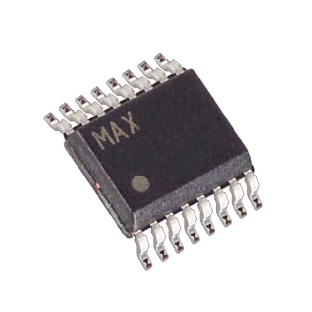
- Part No.:
- MAX9927AEE/V+T
- Manufacturer:
- Analog Devices Inc./Maxim Integrated
- Category:
- Sensor and Detector Interfaces
- Package:
- 16-SSOP (0.154", 3.90mm Width)
- Datasheet:
-
 MAX9927AEE/V+T.pdf
- Description:
- IC VR SENSOR INTERFACE 16QSOP
- Quantity:
- Payment:

- Shipping:

Inventory:2,632
Please send an inquiry. Send us your inquiry, and we will respond immediately.
Product details
Overview
MAX9927AEE/V+T from Maxim Integrated is a dual-channel variable reluctance (VR) sensor interface IC designed for automotive crankshaft and camshaft position/speed sensing. It integrates two precision operational amplifiers with externally configurable gain, adaptive peak threshold detection, zero-crossing circuitry, and open-drain comparator outputs. Operating from 4.5V to 5.5V over −40°C to +125°C, it delivers robust pulse generation from weak or noisy VR signals in engine control units.
For engineers reviewing the MAX9927AEE/V+T datasheet, MAX9927AEE/V+T pinout, MAX9927AEE/V+T application, or MAX9927AEE/V+T equivalent, this page provides verified functional architecture, mode-specific threshold behavior, dual-channel timing alignment, thermal performance data, and automotive-grade supply/ESD robustness metrics essential for ECU signal-chain design.
Technical Context
The MAX9927AEE/V+T implements two independent, fully accessible op-amp channels-each configurable as a differential amplifier using external resistors-enabling precise gain tuning and superior common-mode noise rejection. Its dual zero-crossing comparators generate synchronized output pulses aligned to gear-tooth centers, critical for accurate crank/cam phase measurement.
Adaptive peak threshold operation (Mode A1) uses cycle-by-cycle input signal peak tracking at 33% of prior-cycle amplitude, with an 85ms watchdog timeout that reverts to fixed minimum threshold (20–50mV) during signal loss. Mode B disables adaptation and accepts external threshold voltage (1.5V to VCC−1.1V) for firmware-controlled algorithms.
Key Specifications
| Parameter | Value and Actual Design Meaning |
|---|---|
| Supply Voltage | 4.5V to 5.5V - supports direct connection to automotive 5V rail with ±5% tolerance. |
| Operating Temperature | −40°C to +125°C - qualified for under-hood engine control module placement. |
| Supply Current | 4.7mA (typ), 10mA (max) - enables low-power ECU designs without compromising noise immunity. |
| Input Offset Voltage | 0.5mV (max), 5µV/°C drift - ensures stable small-signal amplification across full temperature range. |
| CMRR | 75dB (min), 102dB (typ) - rejects common-mode noise from ignition systems and alternators. |
| Propagation Delay | 150ns (adaptive path), 50ns (zero-crossing path) - enables sub-degree crank angle resolution at 10,000 RPM. |
| Adaptive Threshold Accuracy | 33% of prior-cycle peak - dynamically scales detection threshold to maintain signal integrity across varying engine speeds. |
Pinout & Package
MAX9927AEE/V+T is housed in a 16-pin QSOP package (5.3mm × 10.2mm, 1.0mm height) with gull-wing leads, RoHS-compliant and automotive-qualified (AEC-Q100 Grade 0).
| Pin/Terminal | Circuit Role | Design Meaning |
|---|---|---|
| IN1+, IN1− | Differential Input Channel 1 | Accepts legacy single-ended or modern differential VR sensor signals; high-impedance CMOS inputs. |
| IN2+, IN2− | Differential Input Channel 2 | Independent second channel for quadrature or dual-sensor configurations; no internal coupling to Channel 1. |
| BIAS1, BIAS2 | Input Bias Reference Inputs | Accept external VCC/2 divider or connect to GND for Mode A2 internal 2.5V reference; bypass required. |
| COUT1, COUT2 | Open-Drain Comparator Outputs | Drive microcontroller GPIOs directly; require 10kΩ pull-up to VPULLUP (up to 5.5V); support mixed-voltage interfaces. |
| EXT1, EXT2 | External Threshold Inputs | Enable Mode B operation; accept 1.5V–(VCC−1.1V) DC voltage for custom threshold algorithms. |
| INT_THRS1, INT_THRS2 | Internal Adaptive Threshold Enable | Logic-controlled activation of adaptive peak detection per channel; tied to VCC for Mode A1. |
| VCC, GND | Power Supply Pins | Support 4.5V–5.5V operation; require parallel 0.1µF + 1µF + 10nF ceramic decoupling per channel. |
| OUT1, OUT2 | Amplifier Output Terminals | Provide buffered op-amp outputs for diagnostic monitoring or secondary signal processing paths. |
Key Features
| Feature | Design Value |
|---|---|
| Dual independent op-amp channels | Each with full terminal access (IN+, IN−, OUT, BIAS) enables flexible gain configuration and diagnostic visibility. |
| Adaptive peak threshold with watchdog | 85ms timeout resets threshold to 20–50mV minimum, ensuring recovery after intermittent sensor disconnection. |
| Zero-crossing detection per channel | Generates timing-accurate pulses referenced to BIAS voltage, delivering <±0.5° crank angle error at 8000 RPM. |
| Automotive-grade thermal performance | θJA = 103.7°C/W (QSOP); continuous operation up to +125°C ambient with 150°C junction limit. |
| Robust input protection | Withstands ±40mA input current and −0.3V to (VCC+0.3V) pin voltage range, surviving load-dump transients. |
Applications
| Camshaft Position Sensing | Crankshaft Position Sensing |
|---|---|
|
Use Scenario: Detecting cam lobe position in overhead-cam gasoline engines to enable variable valve timing (VVT) actuation. IC Role / Device Role / Timing Role: Dual-channel interface synchronizing cam and crank signals for cylinder identification and ignition timing. Use Value: Enables <1° cam phase resolution via zero-crossing alignment to gear tooth center, supporting tight VVT control windows. |
Use Scenario: Measuring flywheel tooth passage in diesel engine control units for fuel injection timing and speed regulation. IC Role / Device Role / Timing Role: Primary crank signal conditioner converting low-amplitude VR output into clean, jitter-free digital pulses. Use Value: Adaptive threshold maintains reliable pulse detection down to 20mV peak input at idle, eliminating missed-tooth errors. |
| Transmission Input Speed Sensing | Quadrature-Based Direction Detection |
|
Use Scenario: Monitoring geartrain speed in automatic transmissions for torque converter lockup and shift scheduling. IC Role / Device Role / Timing Role: High-noise-immunity VR interface operating near high-current solenoid drivers and PWM inverters. Use Value: 75dB+ CMRR suppresses 10kHz–1MHz switching noise, preventing false edge detection during aggressive shifting. |
Use Scenario: Determining rotational direction in dual-VRS setups used in high-performance turbocharged engines. IC Role / Device Role / Timing Role: Dual-channel timing alignment enabling phase comparison between COUT1 and COUT2 outputs. Use Value: Sub-50ns inter-channel propagation delay matching ensures unambiguous direction resolution at >15,000 RPM. |
Equivalent & Alternatives
The following parts are listed as comparable options for similar VR sensor interface applications.
| Alternative Part | Technical Difference | Application Difference | Selection Advice |
|---|---|---|---|
| MAX9926UAEE/V+ | Dual-channel with integrated matched resistors (fixed 1V/V gain); includes DIRN output for quadrature direction. | Lacks external gain flexibility; optimized for legacy VR sensors where gain stability > tunability. | Select when using differential VR sensors requiring minimal external components and directional feedback. |
| NCV7240DR2G | Single-channel VR interface with integrated LDO (5.0V); lower supply current (3.2mA typ); no adaptive threshold. | Relies on fixed hysteresis; less effective on weak or distorted VR waveforms at low RPM. | Select for cost-sensitive single-sensor applications where adaptive threshold is not required. |
Compared with MAX9927AEE/V+T, MAX9926UAEE/V+ offers simpler layout but less gain flexibility, while NCV7240DR2G reduces BOM count at the expense of dynamic threshold adaptation-making MAX9927AEE/V+T optimal for multi-sensor, high-accuracy engine timing systems.
Availability
MAX9927AEE/V+T is available at Aetrix Electronics and suitable for automotive engine control units, transmission control modules, and vehicle speed sensing applications requiring stable component supply across extended temperature and lifecycle requirements.
Supply support for MAX9927AEE/V+T includes scheduled delivery planning, volume procurement assistance, BOM continuity management, traceable sourcing, and lifecycle availability coordination for OEM customers, industrial embedded developers, connected-device designers, and electronics production programs.
Manufacturer
Maxim Integrated (now part of Analog Devices) designs high-performance analog and mixed-signal ICs for automotive, industrial, and communications markets, with emphasis on signal integrity and reliability.
The MAX9924–MAX9927 family was engineered specifically for automotive variable reluctance sensor interfacing, prioritizing noise immunity, adaptive thresholding, and AEC-Q100 compliance in harsh under-hood environments.
FAQ
What is the function of the EXT1 and EXT2 pins on the MAX9927AEE/V+T?
The EXT1 and EXT2 pins on the MAX9927AEE/V+T serve as external threshold inputs for Mode B operation. When INT_THRS1 or INT_THRS2 is grounded, the corresponding channel disables adaptive peak detection and uses the voltage applied to EXT1 or EXT2 (1.5V to VCC−1.1V) as the comparator threshold. This allows firmware-based algorithms-such as PWM-filtered thresholds-to dynamically adjust sensitivity per channel without hardware changes. The MAX9927AEE/V+T's input leakage of ≤10µA ensures minimal loading of external threshold sources.
How does the MAX9927AEE/V+T handle signal dropout or intermittent sensor connection?
The MAX9927AEE/V+T incorporates an 85ms watchdog timer per channel that monitors adaptive peak threshold activity. If no valid zero-crossing or peak event occurs within this window, the threshold automatically drops to the fixed minimum level (20–50mV), enabling immediate pulse recovery upon signal restoration. This behavior-verified in electrical characteristics tables-is critical for maintaining engine synchronization during transient sensor faults. The MAX9927AEE/V+T sustains this recovery capability across −40°C to +125°C without recalibration.
Can the MAX9927AEE/V+T be used with single-ended VR sensors?
Yes, the MAX9927AEE/V+T supports both differential and single-ended VR sensors. For single-ended use, connect the sensor's hot lead to IN1+ (or IN2+) and its ground/shield to IN1− (or IN2−), while referencing BIAS1/BIA2 to VCC/2. The device's rail-to-rail input op amps and ≥75dB CMRR reject common-mode noise from chassis ground loops. Verified application circuits (Figures 6–7) confirm stable operation with 50mV–2V peak single-ended signals-making MAX9927AEE/V+T compatible with legacy VR pickups without adapter hardware.
What is the purpose of the OUT1 and OUT2 pins on the MAX9927AEE/V+T?
The OUT1 and OUT2 pins on the MAX9927AEE/V+T provide buffered operational amplifier outputs for each channel, exposing the amplified VR signal before comparator decision. These outputs enable real-time diagnostic monitoring (e.g., oscilloscope verification of signal integrity), feed-forward control loops, or secondary processing stages. Unlike COUT1/COUT2, OUT1/OUT2 are not open-drain and swing rail-to-rail-supporting direct connection to ADC inputs or analog comparators. Their availability distinguishes MAX9927AEE/V+T from fixed-gain alternatives like MAX9926UAEE/V+.
Does the MAX9927AEE/V+T require external resistors for gain setting?
Yes, the MAX9927AEE/V+T requires four external precision resistors per channel to configure differential amplifier gain, as it does not integrate matched resistors like the MAX9924/MAX9926. Gain is set by the ratio RF/RIN, with typical configurations achieving 1V/V to 10V/V. The device's input bias current (≤6nA) and offset voltage (≤3mV) ensure accuracy even with 100kΩ-level resistor values. Layout guidelines specify symmetric routing and ground-plane isolation to preserve CMRR-validated in MAX9927AEE/V+T's 75dB minimum specification.
MAX9927AEE/V+T Specifications
- Product attributes
- Attribute value
- Manufacturer:
- Analog Devices Inc./Maxim Integrated
- Package/Case:
- 16-SSOP (0.154", 3.90mm Width)
- Series:
- -
- Packaging:
- Tape & Reel (TR)
- Product Status:
- Active
- Programmable:
- Not Verified
- Type:
- Sensor Interface
- Input Type:
- Differential
- Output Type:
- Logic
- Current - Supply:
- 10 mA
- Operating Temperature:
- -40°C ~ 125°C
- Grade:
- Automotive
- Qualification:
- AEC-Q100
- Mounting Type:
- Surface Mount
- Supplier Device Package:
- 16-QSOP
MAX9927AEE/V+T FAQ
1.How can I place an order for MAX9927AEE/V+T through Aetrix?
Please submit a Request for Quotation (RFQ) for MAX9927AEE/V+T on Aetrix. Our sales agent will provide a competitive quotation and guide you through the order confirmation once you accept the terms.
2.Are the price and stock information for MAX9927AEE/V+T reliable?
The price and inventory of MAX9927AEE/V+T are updated periodically and may fluctuate due to market conditions. Stock and pricing data are typically refreshed every 24 hours. Quotation validity for MAX9927AEE/V+T is usually 5 days.
3.What payment methods are accepted for MAX9927AEE/V+T?
We accept Wire Transfer, PayPal, Credit Card, Western Union, MoneyGram, and Escrow for MAX9927AEE/V+T transactions.
Note: Certain payment methods may incur a processing fee.
4.How is shipping managed for MAX9927AEE/V+T?
MAX9927AEE/V+T orders can be shipped via leading logistics carriers, including DHL, UPS, FedEx, TNT, or Registered Mail.
Once your MAX9927AEE/V+T order is processed, you will receive an email with the shipment details and tracking number.
Note: Tracking information may take up to 24 hours to appear. Express delivery typically takes 3–5 business days.
5.How can I obtain technical support or documentation for MAX9927AEE/V+T?
For technical support, including MAX9927AEE/V+T datasheets, pinout diagrams, or application guidance, please contact our engineering support team. They can provide detailed documentation and assistance for your MAX9927AEE/V+T requirements.
6.How does Aetrix verify that MAX9927AEE/V+T is sourced from the original manufacturer or authorized distributors?
All MAX9927AEE/V+T products on Aetrix are procured from qualified distributors and authorized channels. Our dedicated quality assurance team conducts strict verification, including traceability checks and, if necessary, third-party testing. This ensures that MAX9927AEE/V+T meets industry standards.
7.What is the process for return or replacement of MAX9927AEE/V+T?
All MAX9927AEE/V+T units undergo pre-shipment inspection (PSI). If there is an issue with MAX9927AEE/V+T, returns or replacements are accepted under the following conditions:
1.Quantity discrepancies, incorrect items, or visible external defects (such as breakage or corrosion), acknowledged by Aetrix.
2.The issue is reported within 90 days of delivery.
3.The MAX9927AEE/V+T part is unused and in its original packaging.
Return procedure for MAX9927AEE/V+T:
1.Submit a request within 90 days.
2.Obtain a Return Material Authorization (RMA) from Aetrix.
MAX9927AEE/V+T Tags

-
RE46C100S8TF
Microchip Technology

-
XTR111AIDRCR
Texas Instruments

-
XTR111AIDGQR
Texas Instruments

-
XTR117AIDGKR
Texas Instruments
-
XTR111AIDGQT
Texas Instruments

-
XTR115UA/2K5
Texas Instruments
-
MAX14626ETT+T
Analog Devices Inc./Maxim Integrated
-
XTR116UA/2K5
Texas Instruments
-
XTR115U/2K5
Texas Instruments
-
XTR116U/2K5
Texas Instruments

-
PGA308AIDGSR
Texas Instruments
-
XTR300AIRGWR
Texas Instruments
Tech Hub

A practical engineering guide to 3.3V and 5V logic compatibility, input thresholds, resistor dividers, translator ICs, MOSFET level shifting, I2C pull-ups, timing limits and power-sequencing risks.

The 74HC595 uses push-pull logic outputs, while the TPIC6B595 uses 50 V open-drain DMOS sinks for higher-power loads. This guide compares timing, current limits, 3.3 V interfacing, load wiring, thermal…

The 74HC595 converts serial data into eight stable parallel outputs. This guide covers pin functions, shift and storage timing, OE and MR behavior, drive-current limits, cascading, voltage compatibilit…

A technical comparison of level-sensitive latches and edge-triggered flip-flops, covering timing windows, setup and hold limits, master–slave operation, time borrowing, race-through, HDL inference and…

A D latch stores one bit while Enable controls when data can pass. This reference covers gate-level operation, truth tables, transparency, setup and hold timing, LE versus OE, common ICs and practical …

An SR latch stores one bit through cross-coupled feedback. This engineering reference covers NOR and NAND implementations, truth tables, forbidden-state recovery, gated operation, switch debouncing, fa…

Latch circuits retain one bit through feedback. This technical reference covers SR and D latches, truth tables, transparency, timing limits, latch-versus-flip-flop behavior, applications and common log…

An engineering guide to LED driver operation, constant-current and constant-voltage outputs, linear and switching topologies, dimming, IC selection, calculations, replacement compatibility, and fault c…

Operational amplifier guide covering op amp basics, feedback, ideal vs real op amps, common configurations, buffer circuits, offset, bias current, gain-bandwidth, slew rate, rail-to-rail limits and sel…

Jumper cables guide covering safe connection order, red and black clamp placement, final ground connection, cable gauge, length, clamp quality, copper vs CCA cables, jump starter comparison and battery…


