
 My Inquiry
 My Account


Analog Devices Inc./Maxim Integrated MAX9947ETE+
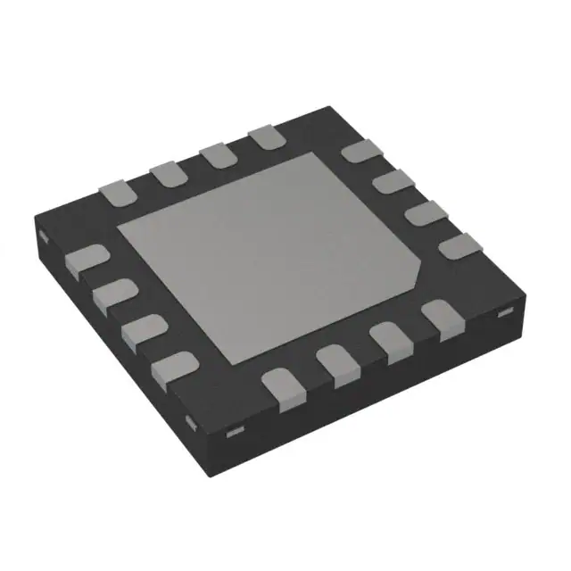
- Part No.:
- MAX9947ETE+
- Manufacturer:
- Analog Devices Inc./Maxim Integrated
- Category:
- RF Transceiver ICs
- Package:
- 16-WFQFN Exposed Pad
- Datasheet:
-
 MAX9947ETE+.pdf
- Description:
- IC RF TXRX AISG 16QFN
- Quantity:
- Payment:

- Shipping:

Inventory:162
Please send an inquiry. Send us your inquiry, and we will respond immediately.
Product details
Overview
The MAX9947ETE+ from Maxim Integrated is an AISG-compliant, fully integrated OOK transceiver for antenna interface control in base station and tower-mounted equipment. It operates at 2.176MHz with ±100ppm frequency stability, delivers +7dBm to +12dBm transmitter output power, supports 9.6/38.4/115.2kbps data rates, and features AutoDirection™ output for RS-485 bus arbitration in remote radio units.
For engineers reviewing the MAX9947ETE+ datasheet, MAX9947ETE+ pinout, MAX9947ETE+ application, or MAX9947ETE+ equivalent, this page provides verified functional context, validated pin roles, confirmed AISG protocol compliance, real-world dynamic range (-15dBm to +5dBm), and precise thermal and supply specifications for tower-mount deployment.
Technical Context
The MAX9947ETE+ integrates independent OOK modulator and demodulator paths with matched 200kHz-bandwidth bandpass filters centered at 2.176MHz. Its receiver achieves -15dBm typical sensitivity (±3dB) into 50Ω, while the transmitter uses external RES/BIAS resistors to set output level across +7dBm to +12dBm with guaranteed AISG spectrum mask compliance per 3GPP TS 25.461.
Direction detection is implemented via internal state machine monitoring both RXIN and TXIN, asserting DIR high only during valid receive events - eliminating need for microcontroller-based arbitration. Clock synchronization uses 8.704MHz crystal (±30ppm) or SYNCOUT-distributed clock, with VL and VCC supplies independently configurable from 1.6V–5.5V and 3.0V–5.5V respectively.
Key Specifications
| Parameter | Value and Actual Design Meaning |
|---|---|
| Operating Frequency | 2.176MHz carrier with ±100ppm stability - meets AISG spectral mask timing requirements for reliable tower-base communication. |
| Receiver Input Range | -15dBm to +5dBm (50Ω) - supports wide dynamic signal levels from weak remote sensors to strong local couplings without external attenuation. |
| Transmitter Output Power | +7dBm to +12dBm adjustable via external resistors - compensates for feeder cable loss and filter insertion loss up to 5dB. |
| Data Rates Supported | 9.6kbps, 38.4kbps, 115.2kbps - full AISG v2.x/3.x compatibility with automatic bit-time duration selection via DIRMD1/DIRMD2 pins. |
| Supply Voltage Ranges | VCC: 3.0V–5.5V; VL: 1.6V–5.5V - enables flexible power domain partitioning between analog and logic sections in mixed-voltage systems. |
| Temperature Range | -40°C to +105°C - qualified for outdoor tower-mounted operation under extreme environmental stress. |
| Package | 16-pin TQFN-EP (3mm × 3mm) with exposed pad - provides low thermal resistance (θJA = 57.2°C/W) for sustained RF output in compact enclosures. |
Pinout & Package
MAX9947ETE+ uses a 3mm × 3mm, 16-pin TQFN package with exposed thermal pad (EP) connected to GND. Pin 1 is marked by dot; EP must be soldered to PCB ground plane for optimal thermal performance and EMI suppression.
| Pin/Terminal | Circuit Role | Design Meaning |
|---|---|---|
| 1 (SYNCOUT) | Open-drain clock output | Provides 8.704MHz synchronization signal to slave devices; requires 1kΩ pullup to VCC for proper logic-level drive. |
| 2 (TXIN) | Digital input | Accepts TTL/CMOS-level OOK data stream; VIH/VIL thresholds scale with VL supply voltage. |
| 3 (VL) | Logic supply | Independent 1.6V–5.5V supply for digital I/O; decouples logic noise from analog VCC domain. |
| 4 (RXOUT) | Digital output | Reconstructed OOK data output; VOH/VOL defined relative to VL, capable of driving RS-485 transceiver enable inputs. |
| 5 (DIR) | Direction indicator | Asserts high during RXIN-to-RXOUT data flow; directly controls DE/RE# of RS-485 transceivers like MAX13485E/MAX13486E. |
| 6,7 (DIRMD2, DIRMD1) | Mode select inputs | Set AISG bit-time duration: 00=9.6kbps (104.16µs), 01=38.4kbps (26.04µs), 10=115.2kbps (8.68µs). |
| 8,16 (GND) | Analog/digital ground | Common reference for all analog and digital circuitry; EP must be connected to same ground plane. |
| 9 (RES) | Power-level reference | Resistor divider node setting TXOUT amplitude; voltage range 0.84V–1.5V determines output from +7dBm to +12dBm. |
| 10 (BIAS) | Bias reference | Internal 1.5V reference used with RES to configure output power; requires 1µF bypass capacitor to GND. |
| 11 (RXIN) | RF input | 50Ω-terminated OOK-modulated 2.176MHz input; accepts -15dBm to +5dBm signals with integrated bandpass filtering. |
| 12 (TXOUT) | RF output | 50Ω-terminated OOK-modulated output; DC-biased at 1.5V for optimal PSRR and emission control. |
| 13 (VCC) | Analog supply | 3.0V–5.5V analog core supply; PSRR >49dB ensures immunity to power rail noise affecting RF performance. |
| 14,15 (XTAL1, XTAL2) | Clock interface | Supports 8.704MHz crystal (XTAL1/XTAL2) or external clock (XTAL1 only, XTAL2=GND); ±30ppm crystal recommended. |
Key Features
| Feature | Design Value |
|---|---|
| AISG-compliant emission profile | Guaranteed conformance to 3GPP TS 25.461 spectrum mask - eliminates need for external filtering in certified base station designs. |
| AutoDirection™ output | Hardware-based DIR assertion synchronized to RXIN activity - removes software arbitration overhead and latency in tower-mounted slave nodes. |
| Variable transmitter output | +7dBm to +12dBm adjustment via two external resistors - enables precise compensation for cable loss, connector mismatch, and filter roll-off. |
| Wide receiver dynamic range | -15dBm to +5dBm input range with 20dB typical dynamic range - accommodates varying signal strengths across multi-element antenna arrays. |
| Independent logic supply (VL) | 1.6V–5.5V VL domain isolated from VCC - allows interfacing with 1.8V, 3.3V, or 5V controllers without level shifters. |
| Crystal or SYNCOUT clock distribution | Single 8.704MHz source can synchronize multiple MAX9947ETE+ devices - reduces BOM count and improves system-wide timing coherence. |
Applications
| Base Station Control Interface | Tower-Mounted Amplifier (TMA) Management |
|---|---|
|
Use Scenario: Bidirectional AISG communication between base station controller and remote radio head over coaxial feeder cable. IC Role / Device Role / Timing Role: Full-duplex OOK transceiver handling physical layer signaling, clock recovery, and direction arbitration without host processor involvement. Use Value: Enables deterministic <11µs receiver propagation delay and hardware-driven DIR output - meeting AISG v3.x timing constraints for real-time antenna tuning commands. |
Use Scenario: Remote configuration and monitoring of tower-mounted amplifiers, RET actuators, and diplexers via AISG v2.x/v3.x protocol. IC Role / Device Role / Timing Role: Slave-side transceiver providing autonomous bus arbitration via DIR pin to manage RS-485 half-duplex link with minimal MCU intervention. Use Value: Eliminates need for dedicated microcontroller firmware to handle RS-485 DE/RE timing - reducing bill-of-materials and firmware validation effort. |
| Antenna Tuning Unit (ATU) Interface | Multi-Band Remote Radio Head (RRH) |
|
Use Scenario: Real-time impedance matching control between baseband unit and active antenna array using AISG-defined tuning parameters. IC Role / Device Role / Timing Role: High-reliability transceiver supporting 115.2kbps data rate with 8.68µs bit time - enabling sub-10ms closed-loop tuning response. Use Value: Delivers ±100ppm frequency stability and -40°C to +105°C operation - ensuring consistent RF performance across temperature gradients in outdoor enclosures. |
Use Scenario: Integration into compact RRH modules requiring low-power, small-footprint AISG connectivity alongside RF front-end components. IC Role / Device Role / Timing Role: Space-optimized transceiver in 3mm × 3mm TQFN package with exposed pad - enabling thermal management in thermally constrained RF module layouts. Use Value: Achieves 1399mW max power dissipation at +70°C with θJA = 57.2°C/W - sustaining full output power in sealed, fanless RRH housings. |
Equivalent & Alternatives
The following parts are listed as comparable options for similar AISG transceiver applications.
| Alternative Part | Technical Difference | Application Difference | Selection Advice |
|---|---|---|---|
| MAX9948ETE+ | Same pinout and electrical specs; includes integrated 50Ω termination resistor network on TXOUT/RXIN - reduces external component count but increases cost and fixed topology. | Preferred where board space is extremely limited and external termination layout is impractical; not suitable for designs requiring variable termination or AC coupling flexibility. | Select MAX9948ETE+ only if eliminating discrete 50Ω terminations justifies higher unit cost and reduced design flexibility. |
| ADL5511ACPZ-R7 | RF detector IC with 2.176MHz bandpass, but no integrated OOK modulator/demodulator or DIR logic - requires external FPGA or MCU for AISG protocol stack and bus arbitration. | Suitable for custom AISG implementations with existing processing resources; lacks hardware AutoDirection™ and synchronous clock distribution capability. | Choose ADL5511ACPZ-R7 only when leveraging existing digital logic for protocol handling and needing higher measurement accuracy over transceiver functionality. |
Compared with MAX9947ETE+, MAX9948ETE+ offers integrated termination at the expense of design adaptability, while ADL5511ACPZ-R7 provides precision RF detection but shifts protocol and arbitration burden to external logic - making MAX9947ETE+ the optimal balance of integration, compliance, and field-deployable robustness.
Availability
MAX9947ETE+ is available at Aetrix Electronics and suitable for base station infrastructure, tower-mounted amplifier (TMA) control, and antenna tuning unit (ATU) applications requiring stable component supply across extended temperature ranges and long product lifecycles.
Supply support for MAX9947ETE+ includes scheduled delivery planning, volume procurement assistance, BOM continuity management, traceable sourcing, and lifecycle availability coordination for OEM customers, industrial embedded developers, connected-device designers, and electronics production programs.
Manufacturer
Maxim Integrated (now part of Analog Devices) is a semiconductor company specializing in high-performance analog, mixed-signal, and RF solutions for communications, industrial, and automotive markets.
The MAX9947ETE+ belongs to Maxim's AISG transceiver product line, engineered specifically for reliable, low-latency antenna interface control in cellular infrastructure - addressing the need for integrated, standards-compliant, and thermally robust RF signaling in outdoor wireless deployments.
FAQ
What is the maximum allowable voltage on the MAX9947ETE+ TXOUT pin?
The MAX9947ETE+ TXOUT pin has absolute maximum rating of (VCC + 0.3V) when shorted to VCC or GND. Under normal operation with 50Ω termination and 2.176MHz OOK modulation, peak-to-peak voltage remains ≤2.52V (corresponding to +12dBm). Exceeding VCC + 0.3V risks permanent damage to the internal output stage of the MAX9947ETE+.
How does the MAX9947ETE+ achieve AISG spectrum compliance without external filters?
The MAX9947ETE+ integrates bandpass filters compliant with AISG emission mask requirements per 3GPP TS 25.461. A 470pF capacitor between RXIN and GND is recommended above 25MHz to ensure full mask compliance - this passive component works with the internal filter structure, not as a standalone solution. The MAX9947ETE+'s transmitter output profile is guaranteed by design when used with the specified external biasing and termination.
Can the MAX9947ETE+ operate with a 3.3V-only supply, or does it require separate VCC and VL rails?
Yes, the MAX9947ETE+ supports single-rail 3.3V operation: connect both VCC and VL to 3.3V. However, its architecture allows independent scaling - VCC may be set to 5.0V for higher TXOUT headroom while VL remains at 3.3V for logic compatibility. This dual-supply flexibility ensures optimal PSRR (>49dB) and noise isolation in the MAX9947ETE+'s analog and digital domains.
What is the purpose of the DIRMD1 and DIRMD2 pins on the MAX9947ETE+?
DIRMD1 and DIRMD2 are mode-select inputs that configure the MAX9947ETE+ for specific AISG data rates: 00 selects 9.6kbps (104.16µs bit time), 01 selects 38.4kbps (26.04µs), and 10 selects 115.2kbps (8.68µs). These pins determine DIR pulse duration and internal timing alignment - critical for meeting AISG v3.x bus arbitration windows. They are internally pulled down, so floating defaults to 9.6kbps mode.
Does the MAX9947ETE+ require an external crystal, or can it use an oscillator?
The MAX9947ETE+ accepts either an 8.704MHz parallel-resonant crystal (with two 40pF load capacitors) or an external 8.704MHz CMOS clock applied to XTAL1 with XTAL2 grounded. Crystal tolerance of ±30ppm is recommended to meet the ±100ppm total frequency stability requirement. Using a precision oscillator simplifies layout but adds cost; crystal solution minimizes BOM and supports multi-device SYNCOUT distribution from one master MAX9947ETE+.
MAX9947ETE+ Specifications
- Product attributes
- Attribute value
- Manufacturer:
- Analog Devices Inc./Maxim Integrated
- Series:
- -
- Package/Case:
- 16-WFQFN Exposed Pad
- Packaging:
- Tube
- Product Status:
- Active
- Programmable:
- Not Verified
- Type:
- TxRx Only
- RF Family/Standard:
- AISG
- Protocol:
- -
- Modulation:
- OOK
- Frequency:
- 2.176MHz
- Data Rate (Max):
- 115.2kbps
- Power - Output:
- 12dBm
- Sensitivity:
- -
- Memory Size:
- -
- Serial Interfaces:
- -
- GPIO:
- -
- Voltage - Supply:
- 3V ~ 5.5V
- Current - Receiving:
- 23mA
- Current - Transmitting:
- 23mA
- Operating Temperature:
- -40°C ~ 85°C
- Grade:
- -
- Qualification:
- -
- Supplier Device Package:
- 16-TQFN (3x3)
MAX9947ETE+ FAQ
1.How can I place an order for MAX9947ETE+ through Aetrix?
Please submit a Request for Quotation (RFQ) for MAX9947ETE+ on Aetrix. Our sales agent will provide a competitive quotation and guide you through the order confirmation once you accept the terms.
2.Are the price and stock information for MAX9947ETE+ reliable?
The price and inventory of MAX9947ETE+ are updated periodically and may fluctuate due to market conditions. Stock and pricing data are typically refreshed every 24 hours. Quotation validity for MAX9947ETE+ is usually 5 days.
3.What payment methods are accepted for MAX9947ETE+?
We accept Wire Transfer, PayPal, Credit Card, Western Union, MoneyGram, and Escrow for MAX9947ETE+ transactions.
Note: Certain payment methods may incur a processing fee.
4.How is shipping managed for MAX9947ETE+?
MAX9947ETE+ orders can be shipped via leading logistics carriers, including DHL, UPS, FedEx, TNT, or Registered Mail.
Once your MAX9947ETE+ order is processed, you will receive an email with the shipment details and tracking number.
Note: Tracking information may take up to 24 hours to appear. Express delivery typically takes 3–5 business days.
5.How can I obtain technical support or documentation for MAX9947ETE+?
For technical support, including MAX9947ETE+ datasheets, pinout diagrams, or application guidance, please contact our engineering support team. They can provide detailed documentation and assistance for your MAX9947ETE+ requirements.
6.How does Aetrix verify that MAX9947ETE+ is sourced from the original manufacturer or authorized distributors?
All MAX9947ETE+ products on Aetrix are procured from qualified distributors and authorized channels. Our dedicated quality assurance team conducts strict verification, including traceability checks and, if necessary, third-party testing. This ensures that MAX9947ETE+ meets industry standards.
7.What is the process for return or replacement of MAX9947ETE+?
All MAX9947ETE+ units undergo pre-shipment inspection (PSI). If there is an issue with MAX9947ETE+, returns or replacements are accepted under the following conditions:
1.Quantity discrepancies, incorrect items, or visible external defects (such as breakage or corrosion), acknowledged by Aetrix.
2.The issue is reported within 90 days of delivery.
3.The MAX9947ETE+ part is unused and in its original packaging.
Return procedure for MAX9947ETE+:
1.Submit a request within 90 days.
2.Obtain a Return Material Authorization (RMA) from Aetrix.
MAX9947ETE+ Tags

-
ESP32-D0WD-V3
Espressif Systems

-
ESP8266EX
Espressif Systems

-
ESP32-S3
Espressif Systems

-
NRF24L01P-R7
Nordic Semiconductor ASA
-
NRF24L01P-R
Nordic Semiconductor ASA

-
ESP32-U4WDH
Espressif Systems

-
DA14531-00000OG2
Renesas
-
ESP32-C6FH4
Espressif Systems

-
DA14531-00000FX2
Renesas
-
NRF24L01P-T
Nordic Semiconductor ASA

-
NRF52810-QCAA-R
Nordic Semiconductor ASA
-
ESP32-S3FN8
Espressif Systems
Tech Hub

A practical engineering guide to 3.3V and 5V logic compatibility, input thresholds, resistor dividers, translator ICs, MOSFET level shifting, I2C pull-ups, timing limits and power-sequencing risks.

The 74HC595 uses push-pull logic outputs, while the TPIC6B595 uses 50 V open-drain DMOS sinks for higher-power loads. This guide compares timing, current limits, 3.3 V interfacing, load wiring, thermal…

The 74HC595 converts serial data into eight stable parallel outputs. This guide covers pin functions, shift and storage timing, OE and MR behavior, drive-current limits, cascading, voltage compatibilit…

A technical comparison of level-sensitive latches and edge-triggered flip-flops, covering timing windows, setup and hold limits, master–slave operation, time borrowing, race-through, HDL inference and…

A D latch stores one bit while Enable controls when data can pass. This reference covers gate-level operation, truth tables, transparency, setup and hold timing, LE versus OE, common ICs and practical …

An SR latch stores one bit through cross-coupled feedback. This engineering reference covers NOR and NAND implementations, truth tables, forbidden-state recovery, gated operation, switch debouncing, fa…

Latch circuits retain one bit through feedback. This technical reference covers SR and D latches, truth tables, transparency, timing limits, latch-versus-flip-flop behavior, applications and common log…

An engineering guide to LED driver operation, constant-current and constant-voltage outputs, linear and switching topologies, dimming, IC selection, calculations, replacement compatibility, and fault c…

Operational amplifier guide covering op amp basics, feedback, ideal vs real op amps, common configurations, buffer circuits, offset, bias current, gain-bandwidth, slew rate, rail-to-rail limits and sel…

Jumper cables guide covering safe connection order, red and black clamp placement, final ground connection, cable gauge, length, clamp quality, copper vs CCA cables, jump starter comparison and battery…


