
 My Inquiry
 My Account


Analog Devices Inc./Maxim Integrated MAX9955BDCCB+D
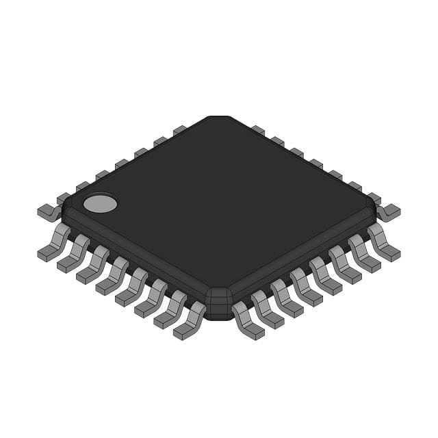
- Part No.:
- MAX9955BDCCB+D
- Manufacturer:
- Analog Devices Inc./Maxim Integrated
- Category:
- Comparators
- Package:
- 64-TQFP Exposed Pad
- Datasheet:
-
 MAX9955BDCCB+D.pdf
- Description:
- IC COMPARATOR 2 GEN PUR 64TQFP
- Quantity:
- Payment:

- Shipping:

Inventory:1,745
Please send an inquiry. Send us your inquiry, and we will respond immediately.
Product details
Overview
The MAX9955BDCCB+D from Maxim Integrated is a high-speed dual comparator/terminator IC designed for automated test equipment (ATE) signal conditioning. It integrates two independent comparators with programmable cable-droop compensation, 55ps input rise/fall time, 190ps minimum pulse width, and dual 50Ω buffered terminators per channel-enabling precise timing capture in DDR3/GDDR4 memory ATE systems.
For engineers reviewing the MAX9955BDCCB+D datasheet, MAX9955BDCCB+D pinout, MAX9955BDCCB+D application, or MAX9955BDCCB+D equivalent, key selection criteria include its -1.1V to +3.6V comparator input range, ±50mA terminator overcurrent protection, die temperature monitoring output, and compatibility with doubly terminated 0.4VP-P CML interfaces.
Technical Context
The MAX9955BDCCB+D implements two fully independent comparator channels, each with differential open-collector outputs, internal 50Ω termination resistors, and separate high/low reference inputs (CHV_/CLV_). Each channel includes dedicated cable-droop compensation inputs (COS_/COL_) with fixed 50ps and 1.5ns time constants for high- and low-frequency peaking.
Its integrated terminator buffers accept DTV_ reference voltage and deliver 50Ω source impedance with ±50mA current limiting and latched OVL flag indication. The device uses bipolar process technology, features an exposed die paddle thermally connected to VEE, and supports die temperature monitoring via the TEMP pin with 10mV/°C slope and 3.52V nominal output at +70°C.
Key Specifications
| Parameter | Value and Actual Design Meaning |
|---|---|
| Comparator Input Range | -1.1V to +3.6V - supports wide-swing ATE signals including DDR3/GDDR4 DQ/DQS levels |
| Terminator Output Impedance | 48Ω to 52Ω - tightly controlled 50Ω buffered source termination for impedance-matched CML links |
| Input Timing Dispersion | ±5ps max match between comparators - ensures sub-10ps channel-to-channel skew in parallel test setups |
| Min Pulse Width | 190ps - enables accurate detection of ultra-short test pulses in high-speed memory characterization |
| Power Dissipation | 850mW per channel at 2Gbps - optimized for thermal management in dense ATE load boards |
| DIE Temperature Range | +50°C to +90°C - specified operating junction range with on-chip TEMP monitor for thermal derating |
| Cable-Droop Compensation | Two independent analog controls (COS_/COL_) - corrects frequency-dependent loss in >2m RG174 test cables |
Pinout & Package
MAX9955BDCCB+D is housed in a 64-pin TQFP-IDP (inverted die paddle) package measuring 10mm × 10mm with 0.5mm pitch. The top-side exposed paddle is internally connected to VEE and provides enhanced thermal dissipation for high-power ATE operation.
| Pin/Terminal | Circuit Role | Design Meaning |
|---|---|---|
| DUT1 / DUT2 | Combined comparator + terminator input | Single node accepts Device-Under-Test signal for simultaneous comparison and buffered termination |
| CH1/NCH1 / CH2/NCH2 | Differential comparator outputs | Open-collector outputs with internal 50Ω termination to VCCOH_; support CML-level signaling |
| CL1/NCL1 / CL2/NCL2 | Differential comparator outputs | Paired with CHx outputs to form full logic decision (see Table 1); require external pull-up or VCCOL_ bias |
| DTV1 / DTV2 | Terminator reference input | Sets DC level of 50Ω buffered output; supports -1.0V to +3.5V programming range |
| COS1/COL1 / COS2/COL2 | Cable-droop compensation controls | Analog inputs adjusting high-frequency (50ps τ) and low-frequency (1.5ns τ) peaking amplitude |
| HYS1 / HYS2 | Hysteresis programming node | Connect resistor to GND to set 0–10mV hysteresis; open = zero hysteresis mode |
| OVL | Overcurrent latch flag | Open-drain output asserting high when either channel exceeds ±50mA buffer current limit |
| TEMP | Die temperature monitor | Analog voltage output scaling 3.52V at +70°C with +10mV/°C coefficient for real-time thermal feedback |
Key Features
| Feature | Design Value |
|---|---|
| Programmable cable-droop compensation | Independent COS_/COL_ inputs enable adaptive correction of transmission-line loss in long test fixtures |
| Low timing dispersion | ±5ps comparator propagation delay match ensures synchronized decision timing across dual channels |
| Dual 50Ω buffered terminators | On-die 50Ω source termination eliminates discrete resistors and improves signal integrity in CML interfaces |
| Hysteresis control (0–10mV) | Resistor-programmable noise immunity prevents false triggering on slow-rising test waveforms |
| Integrated die temperature monitor | TEMP pin delivers calibrated 10mV/°C analog output for closed-loop thermal management in ATE loadboards |
Applications
| DDR3 Memory ATE Channel Interface | GDDR4 Graphics Memory Tester |
|---|---|
Use Scenario: Capturing high-speed DQ/DQS strobes from DDR3 memory devices under test using parallel multi-site test architecture. IC Role / Device Role / Timing Role: Dual-channel comparator/terminator conditions and digitizes memory I/O waveforms while providing matched timing paths and cable-loss compensation. Use Value: Enables <190ps pulse-width detection and ±5ps inter-channel skew control required for DDR3 write-leveling calibration. | Use Scenario: Signal acquisition and threshold validation in GDDR4 graphics memory testers handling >2Gbps data rates. IC Role / Device Role / Timing Role: Provides high-fidelity waveform digitization with integrated 50Ω termination and droop compensation for long probe cabling. Use Value: Reduces discrete component count by eliminating external termination networks and RC equalization circuits. |
| High-Speed SOC Test Head Interface | Automated Memory Parametric Tester |
Use Scenario: Interfacing ASIC test heads to high-speed memory controllers during structural and functional test. IC Role / Device Role / Timing Role: Acts as precision timing capture front-end with programmable hysteresis and temperature-compensated references. Use Value: Supports -1.1V to +3.6V input swing and delivers stable 800mVP-P differential outputs compatible with CML receivers. | Use Scenario: Performing parametric measurements (setup/hold, pulse width, slew rate) on memory I/O pins across temperature and voltage corners. IC Role / Device Role / Timing Role: Serves as calibrated comparator with on-chip TEMP monitoring and OVL fault detection for safe current-limited testing. Use Value: Enables real-time thermal derating and overcurrent shutdown without external sense circuitry. |
Equivalent & Alternatives
The following parts are listed as comparable options for similar dual high-speed comparator/terminator applications.
| Alternative Part | Technical Difference | Application Difference | Selection Advice |
|---|---|---|---|
| MAX9957ETL+ | Same pinout, identical comparator/terminator architecture, but adds integrated multiplexer for single-ended DUT inputs | Supports shared DUT input routing in space-constrained ATE headplates; lacks independent DUT1/DUT2 isolation | Select MAX9957ETL+ when multiplexed input architecture reduces board layer count and routing complexity |
| LMH7322MA/NOPB | Single-channel, no integrated terminator; 2.8ns propagation delay vs. MAX9955BDCCB+D's 0.5ns; no cable-droop or TEMP output | Requires external 50Ω termination and thermal monitoring circuitry; suitable only for lower-speed non-ATE applications | Choose LMH7322MA/NOPB only for cost-sensitive, non-critical timing applications where droop compensation and thermal monitoring are unnecessary |
Compared with MAX9955BDCCB+D, the MAX9957ETL+ offers identical timing performance and thermal monitoring but trades dual independent DUT inputs for input multiplexing-while the LMH7322MA/NOPB lacks integrated termination, cable compensation, and die temperature sensing entirely, requiring significant external support circuitry for ATE use.
Availability
MAX9955BDCCB+D is available at Aetrix Electronics and suitable for high-performance memory ATE, SOC test equipment, and parametric memory characterization systems requiring stable component supply, guaranteed long-term availability, and traceable sourcing.
Supply support for MAX9955BDCCB+D includes scheduled delivery planning, volume procurement assistance, BOM continuity management, traceable sourcing, and lifecycle availability coordination for OEM customers, industrial embedded developers, connected-device designers, and electronics production programs.
Manufacturer
Maxim Integrated (now part of Analog Devices) designs precision analog and mixed-signal ICs for test and measurement, communications, and industrial applications.
The MAX9955BDCCB+D belongs to Maxim's high-speed ATE interface product line, engineered specifically for automated memory test systems requiring sub-nanosecond timing accuracy, integrated signal conditioning, and thermal-aware operation.
FAQ
What is the operating temperature range for the MAX9955BDCCB+D die junction?
The MAX9955BDCCB+D is specified for internal die temperature operation from +50°C to +90°C. Its integrated TEMP pin provides a calibrated analog voltage (3.52V nominal at +70°C, +10mV/°C slope) to monitor actual junction temperature in real time-critical for thermal derating in high-density ATE loadboards where ambient cooling is limited.
How does the MAX9955BDCCB+D implement cable-droop compensation?
The MAX9955BDCCB+D implements cable-droop compensation using two independent analog inputs per channel: COS_ (short-duration boost, 50ps time constant) and COL_ (long-duration boost, 1.5ns time constant). These inputs adjust peaking amplitude in the DUT_ signal path to counteract high-frequency loss in test cables-verified to restore waveform fidelity in 2-meter RG174 configurations as shown in typical operating characteristics.
What is the function of the OVL pin on the MAX9955BDCCB+D?
The OVL pin on the MAX9955BDCCB+D is an open-drain overcurrent flag that latches high when either channel's terminator buffer exceeds ±50mA output current. It remains asserted until the RST pin is pulsed low, which resets the latch and closes the buffer output switch-providing fail-safe current limiting for protection of DUT and tester hardware during abnormal test conditions.
Can the MAX9955BDCCB+D be used with CML logic families?
Yes, the MAX9955BDCCB+D is explicitly designed for compatibility with doubly terminated 0.4VP-P CML interfaces. Its differential open-collector comparator outputs (CH_/NCH_, CL_/NCL_) feature internal 50Ω termination to VCCOH_/VCCOL_, delivering nominal 800mVP-P swing-halving to 400mVP-P when paired with external 50Ω destination termination, matching standard CML receiver thresholds.
What package type and thermal features does the MAX9955BDCCB+D use?
The MAX9955BDCCB+D uses a 64-pin TQFP-IDP (inverted die paddle) package (10mm × 10mm, 0.5mm pitch) with an exposed paddle on the top surface. This paddle is internally connected to VEE and serves as the primary thermal path-enabling efficient heat removal in high-power ATE applications where static power dissipation reaches 850mW per channel at 2Gbps.
MAX9955BDCCB+D Specifications
- Product attributes
- Attribute value
- Manufacturer:
- Analog Devices Inc./Maxim Integrated
- Package/Case:
- 64-TQFP Exposed Pad
- Series:
- -
- Packaging:
- Bulk
- Product Status:
- Active
- Type:
- General Purpose
- Number of Elements:
- 2
- Output Type:
- Complementary
- Voltage - Supply, Single/Dual (±):
- -5.5V ~ -4.75V, 6.75V ~ 7.5V
- :
- 20mV @ 3.3V
- Voltage - Input Offset (Max):
- 25µA @ 7V
- Current - Input Bias (Max):
- -
- Current - Output (Typ):
- 121mA, 174mA
- Current - Quiescent (Max):
- 130.457dB CMRR, 131dB PSRR
- CMRR, PSRR (Typ):
- 650ps
- Propagation Delay (Max):
- 10mV
- Hysteresis:
- 0°C ~ 70°C
- Operating Temperature:
- -
- Grade:
- -
- Qualification:
- Surface Mount
- :
- 64-TQFP-EP (10x10)
MAX9955BDCCB+D FAQ
1.How can I place an order for MAX9955BDCCB+D through Aetrix?
Please submit a Request for Quotation (RFQ) for MAX9955BDCCB+D on Aetrix. Our sales agent will provide a competitive quotation and guide you through the order confirmation once you accept the terms.
2.Are the price and stock information for MAX9955BDCCB+D reliable?
The price and inventory of MAX9955BDCCB+D are updated periodically and may fluctuate due to market conditions. Stock and pricing data are typically refreshed every 24 hours. Quotation validity for MAX9955BDCCB+D is usually 5 days.
3.What payment methods are accepted for MAX9955BDCCB+D?
We accept Wire Transfer, PayPal, Credit Card, Western Union, MoneyGram, and Escrow for MAX9955BDCCB+D transactions.
Note: Certain payment methods may incur a processing fee.
4.How is shipping managed for MAX9955BDCCB+D?
MAX9955BDCCB+D orders can be shipped via leading logistics carriers, including DHL, UPS, FedEx, TNT, or Registered Mail.
Once your MAX9955BDCCB+D order is processed, you will receive an email with the shipment details and tracking number.
Note: Tracking information may take up to 24 hours to appear. Express delivery typically takes 3–5 business days.
5.How can I obtain technical support or documentation for MAX9955BDCCB+D?
For technical support, including MAX9955BDCCB+D datasheets, pinout diagrams, or application guidance, please contact our engineering support team. They can provide detailed documentation and assistance for your MAX9955BDCCB+D requirements.
6.How does Aetrix verify that MAX9955BDCCB+D is sourced from the original manufacturer or authorized distributors?
All MAX9955BDCCB+D products on Aetrix are procured from qualified distributors and authorized channels. Our dedicated quality assurance team conducts strict verification, including traceability checks and, if necessary, third-party testing. This ensures that MAX9955BDCCB+D meets industry standards.
7.What is the process for return or replacement of MAX9955BDCCB+D?
All MAX9955BDCCB+D units undergo pre-shipment inspection (PSI). If there is an issue with MAX9955BDCCB+D, returns or replacements are accepted under the following conditions:
1.Quantity discrepancies, incorrect items, or visible external defects (such as breakage or corrosion), acknowledged by Aetrix.
2.The issue is reported within 90 days of delivery.
3.The MAX9955BDCCB+D part is unused and in its original packaging.
Return procedure for MAX9955BDCCB+D:
1.Submit a request within 90 days.
2.Obtain a Return Material Authorization (RMA) from Aetrix.
MAX9955BDCCB+D Tags

-
LM2903DR
Texas Instruments

-
LM339DR
Texas Instruments

-
LM339PWR
Texas Instruments

-
LM393DT
STMicroelectronics
-
LM2901PWR
Texas Instruments
-
LM2903DT
STMicroelectronics
-
LM393DR
Texas Instruments
-
LM239DR
Texas Instruments
-
LM339APWR
Texas Instruments

-
LM2903P
Texas Instruments
-
LM393ADR
Texas Instruments
-
NCX2200GMAZ
NXP USA Inc.
Tech Hub

An engineering guide to LED driver operation, constant-current and constant-voltage outputs, linear and switching topologies, dimming, IC selection, calculations, replacement compatibility, and fault c…

Operational amplifier guide covering op amp basics, feedback, ideal vs real op amps, common configurations, buffer circuits, offset, bias current, gain-bandwidth, slew rate, rail-to-rail limits and sel…

Jumper cables guide covering safe connection order, red and black clamp placement, final ground connection, cable gauge, length, clamp quality, copper vs CCA cables, jump starter comparison and battery…

LDO regulator guide covering low dropout voltage, power dissipation, thermal design, PSRR, output noise, capacitor stability, adjustable LDO circuits, LDO vs buck converter and datasheet selection chec…

Conditional Access Module guide covering CAM meaning, CI/CI+ interface, smart card authorization, DVB security workflow, TV and set-top box compatibility, internal electronics, ESD protection, connecto…

Guide to electronic component obsolescence covering EOL risk, PCN/PDN notices, last-time buy planning, replacement options, form-fit-function validation, counterfeit risk and BOM lifecycle management.

18650 battery guide covering lithium-ion cell basics, 3.6V/3.7V voltage, 4.2V charging, mAh and Wh capacity, protected cells, chargers, BMS, series-parallel packs, holders, welding and sourcing checks.…

Hall effect sensor guide covering working principle, linear and digital sensors, Arduino circuits, current sensing, speed detection, automotive applications, A3144 examples, signal filtering and datash…

Product Change Notification guide for electronic components, covering PCN meaning, PCN vs PDN/EOL, common change types, risk levels, form-fit-function review, engineering validation, BOM control, LTB/L…

A practical guide to blend door actuators, covering HVAC function, symptoms, location, AC and heater issues, reset and calibration, replacement cost, electrical diagnosis, compatibility checks, and rep…


