
 My Inquiry
 My Account


Analog Devices Inc./Maxim Integrated MAXQ1103-ENS+
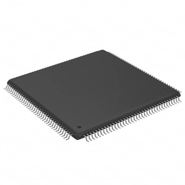
- Part No.:
- MAXQ1103-ENS+
- Manufacturer:
- Analog Devices Inc./Maxim Integrated
- Category:
- Microcontrollers
- Package:
- 144-TQFP
- Datasheet:
-
 MAXQ1103-ENS+.pdf
- Description:
- IC MCU 32BIT 512KB FLASH 144TQFP
- Quantity:
- Payment:

- Shipping:

Inventory:1,697
Please send an inquiry. Send us your inquiry, and we will respond immediately.
Product details
Overview
MAXQ1103-ENS+ from Maxim Integrated is a DeepCover™ secure microcontroller featuring a 32-bit MAXQ30 RISC core, 512KB internal flash, 32KB SRAM (including 1KB battery-backed NV SRAM), hardware cryptographic accelerators for ECDSA/DSA/RSA/SHA-256/3DES, and rapid zeroization triggered by tamper sensors. It operates from -40°C to +85°C in 144-pin TQFP and targets EMV banking terminals and PCI-compliant secure transaction systems.
For engineers reviewing the MAXQ1103-ENS+ datasheet, MAXQ1103-ENS+ pinout, MAXQ1103-ENS+ application, or MAXQ1103-ENS+ equivalent, key selection considerations include FIPS 140-2 Level 3 certification readiness, dual-voltage operation (1.8V core / 3.3V I/O), ISO 7816 UART support, USB device controller with four endpoints, and tamper-responsive rapid zeroization capability.
Technical Context
The MAXQ1103-ENS+ integrates a pipelined 32-bit MAXQ30 RISC core running DC to 25MHz (≈1 MIPS/MHz), with three independent data pointers and 16×32-bit accumulators. Its security architecture includes a secure memory protection unit, triple-DES encrypted external memory bus, and unresettable true-time clock for timestamping and expiration enforcement.
Cryptographic acceleration is implemented via dedicated hardware blocks: 2048-bit modulo arithmetic accelerator for RSA/DSA, SHA engine supporting SHA-1/224/256, DES/3DES engine, and FIPS 186-2–compliant true hardware RNG. Tamper detection uses on-die high/low temperature sensors and user-defined self-destruct inputs (SDI[1:7]).
Key Specifications
| Parameter | Value and Actual Design Meaning |
|---|---|
| Core Architecture | 32-bit MAXQ30 RISC, single-cycle execution for 34 instructions, 16-bit instruction word |
| Operating Frequency | DC to 25MHz - enables deterministic real-time response up to 25MIPS |
| Memory | 512KB flash (code/data), 32KB SRAM (1KB battery-backed), supports up to 8MB external memory via word-wide bus |
| Crypto Acceleration | Hardware ECDSA (160/192/256-bit), RSA/DSA (1024/2048-bit), SHA-1/224/256, 3DES |
| Tamper Response | Rapid zeroization of keys and user data upon out-of-range voltage/temperature or SDI activation |
| Power Supply | Dual-rail: 1.8V core (VDD), 3.3V I/O (VDDIO), 3V battery backup (VBAT); ultra-low 150nA battery leakage |
| Security Certifications | Designed to meet FIPS 140-2 Level 3, ITSEC E3 High, and Common Criteria requirements |
Pinout & Package
MAXQ1103-ENS+ is housed in a 144-pin Thin Quad Flat Package (TQFP) with 0.5mm pitch, thermally enhanced for industrial temperature operation (-40°C to +85°C). The package includes dedicated tamper-sensing pins (SDI[1:7]), dual power domains (VDD/VDDIO/VBAT), and segregated analog/digital ground planes (GND/GND2).
| Pin/Terminal | Circuit Role | Design Meaning |
|---|---|---|
| SDI[1:7] | User-defined self-destruct input | Active-high signals triggering immediate zeroization of cryptographic keys and sensitive RAM |
| HFXIN/HFXOUT | High-frequency crystal oscillator interface | Supports external 1–20MHz crystal for precise clock source; internal PLL generates 55MHz core clock |
| USB D+/D- | USB 2.0 Full-Speed differential pair | Integrated USB device controller with four endpoint buffers; no external transceiver required |
| PCS1/PCS1N, PCS2/PCS2N | Programmable chip select outputs | Enable banked access to external memory or peripherals with configurable timing and polarity |
| ISO7816 I/O | Smart card interface (T=0/T=1) | Dedicated UART with FIFO and two physically separate buses for dual smart card readers |
Key Features
| Feature | Design Value |
|---|---|
| Rapid zeroization circuitry | Sub-microsecond erasure of all volatile cryptographic keys and user data upon tamper event |
| Triple-DES encrypted external bus | Prevents eavesdropping on off-chip memory transactions using hardware-enforced 3DES encryption |
| True hardware RNG | FIPS 186-2–certifiable random number generation with entropy sourced from analog noise circuits |
| Unresettable RTC | Self-imposes expiration dates on stored credentials and provides cryptographically verifiable timestamps |
| Dual-voltage I/O | 3.3V-tolerant I/O with 1.8V core enables low-power operation while interfacing with legacy 3.3V peripherals |
Applications
| EMV® Banking Terminals | PCI PTS-Compliant PIN Pads |
|---|---|
Use Scenario: Secure processing of chip-and-PIN card transactions in ATMs and point-of-sale terminals. IC Role / Device Role / Timing Role: Root-of-trust microcontroller executing EMV kernel, managing cryptographic keys, and enforcing transaction integrity. Use Value: FIPS 140-2 Level 3–aligned tamper detection and rapid zeroization prevent physical extraction of master keys during skimming attacks. | Use Scenario: Real-time encryption and validation of PIN entries in payment acceptance devices. IC Role / Device Role / Timing Role: Secure co-processor handling PIN block generation, AES/3DES encryption, and ISO 7816 smart card communication. Use Value: Hardware-accelerated ECDSA and SHA-256 enable fast certificate-based authentication without software overhead. |
| Secure Access Control Systems | Electronic Signature Generators |
Use Scenario: Biometric template storage and cryptographic signing for physical access badges or logical network logins. IC Role / Device Role / Timing Role: Trusted execution environment for biometric matching algorithms and private key operations. Use Value: Battery-backed NV SRAM preserves biometric templates across power loss; tamper sensors disable access upon enclosure breach. | Use Scenario: Creation of legally binding digital signatures for document signing in regulated industries. IC Role / Device Role / Timing Role: Cryptographic signing engine performing ECDSA/DSA with hardware-accelerated modulo arithmetic. Use Value: 2048-bit RSA and 256-bit ECDSA signing completed in milliseconds-enabling high-throughput signature generation. |
Equivalent & Alternatives
The following parts are listed as comparable options for similar secure microcontroller applications.
| Alternative Part | Technical Difference | Application Difference | Selection Advice |
|---|---|---|---|
| MAXQ1102-ENS+ | Same MAXQ30 core and security features, but 256KB flash and 16KB SRAM; lacks USB controller | Suitable for cost-sensitive, non-USB embedded security modules with lower memory footprint | Select when USB connectivity is unnecessary and BOM cost reduction is prioritized over peripheral count |
| ST33TPHF2ES | ARM SecurCore SC300 core, 384KB flash, certified to Common Criteria EAL5+, no rapid zeroization circuitry | Targeted at smart card controllers and trusted platform modules requiring long-term CC certification stability | Select when formal CC EAL5+ certification is mandatory and rapid zeroization is secondary to audit trail integrity |
Compared with MAXQ1103-ENS+, the MAXQ1102-ENS+ reduces memory and removes USB but retains identical tamper response and crypto acceleration, while the ST33TPHF2ES offers stronger formal certification at the expense of zeroization speed and hardware RNG assurance.
Availability
MAXQ1103-ENS+ is available at Aetrix Electronics and suitable for EMV banking terminals, PCI PTS-compliant PIN pads, and secure access control systems requiring stable component supply, long-lifecycle support, and traceable RoHS-compliant sourcing.
Supply support for MAXQ1103-ENS+ includes scheduled delivery planning, volume procurement assistance, BOM continuity management, traceable sourcing, and lifecycle availability coordination for OEM customers, industrial embedded developers, connected-device designers, and electronics production programs.
Manufacturer
Maxim Integrated (now part of Analog Devices) designs high-performance analog and mixed-signal ICs for industrial, communications, computing, and consumer applications.
The MAXQ1103-ENS+ belongs to the DeepCover® secure microcontroller product line, engineered specifically for applications demanding physical tamper resistance, cryptographic agility, and regulatory compliance in financial transaction and identity verification systems.
FAQ
What security certifications does the MAXQ1103-ENS+ support?
The MAXQ1103-ENS+ is designed to meet FIPS 140-2 Level 3, ITSEC E3 High, and Common Criteria certification requirements. Its architecture includes tamper-detection sensors, rapid zeroization, encrypted memory buses, and certified cryptographic engines - all essential for achieving these standards. While final certification is granted per implementation, the MAXQ1103-ENS+ provides the foundational hardware capabilities required for evaluation and validation against those criteria.
Does the MAXQ1103-ENS+ include a hardware random-number generator?
Yes, the MAXQ1103-ENS+ integrates a true hardware random-number generator (RNG) compliant with FIPS 186-2. It derives entropy from analog circuit noise and is directly accessible via dedicated registers. This RNG is used internally for key generation and can be accessed by firmware to seed cryptographic operations - a critical feature for the MAXQ1103-ENS+'s role in secure key establishment and non-repudiation.
Can the MAXQ1103-ENS+ operate with both 1.8V and 3.3V supplies simultaneously?
Yes, the MAXQ1103-ENS+ supports dual-supply operation: VDD = 1.8V powers the core logic, while VDDIO = 3.3V powers the I/O banks. This allows low-power core execution while maintaining compatibility with standard 3.3V peripherals and interfaces such as USB and ISO 7816. The MAXQ1103-ENS+ also supports 5V-tolerant I/O pins, simplifying integration into mixed-voltage systems.
What is the purpose of the SDI[1:7] pins on the MAXQ1103-ENS+?
The SDI[1:7] pins on the MAXQ1103-ENS+ are user-defined self-destruct inputs that trigger immediate rapid zeroization of all cryptographic keys and sensitive user data when asserted. These inputs can be connected to external tamper switches, enclosures, or sensor outputs. Their activation bypasses software control - ensuring that even if firmware is compromised, physical intrusion still results in irreversible key erasure on the MAXQ1103-ENS+.
Does the MAXQ1103-ENS+ support external memory expansion?
Yes, the MAXQ1103-ENS+ supports up to 8MB of external program and data memory via a dedicated word-wide memory bus with programmable wait states. This interface includes PCS1/PCS1N and PCS2/PCS2N chip selects, AD[19:0] address lines, and ED[31:0] data lines. The MAXQ1103-ENS+'s memory management unit (MMU) and secure encryptor/decryptor ensure protected, authenticated access to off-chip memory - extending secure storage beyond its 512KB internal flash.
MAXQ1103-ENS+ Specifications
- Product attributes
- Attribute value
- Manufacturer:
- Analog Devices Inc./Maxim Integrated
- Package/Case:
- 144-TQFP
- Series:
- DeepCover®
- Packaging:
- Tray
- Product Status:
- Active
- Programmable:
- Not Verified
- Core Processor:
- MAXQ30
- Core Size:
- 32-Bit Single-Core
- Speed:
- 25MHz
- Connectivity:
- UART/USART, USB
- Peripherals:
- WDT
- Number of I/O:
- 32
- Program Memory Size:
- 512KB (512K x 8)
- Program Memory Type:
- FLASH
- EEPROM Size:
- -
- RAM Size:
- 32K x 8
- Voltage - Supply (Vcc/Vdd):
- 1.8V, 3.3V
- Data Converters:
- -
- Oscillator Type:
- Internal
- Operating Temperature:
- -40°C ~ 85°C (TA)
- Grade:
- -
- Qualification:
- -
- Mounting Type:
- Surface Mount
- Supplier Device Package:
MAXQ1103-ENS+ FAQ
1.How can I place an order for MAXQ1103-ENS+ through Aetrix?
Please submit a Request for Quotation (RFQ) for MAXQ1103-ENS+ on Aetrix. Our sales agent will provide a competitive quotation and guide you through the order confirmation once you accept the terms.
2.Are the price and stock information for MAXQ1103-ENS+ reliable?
The price and inventory of MAXQ1103-ENS+ are updated periodically and may fluctuate due to market conditions. Stock and pricing data are typically refreshed every 24 hours. Quotation validity for MAXQ1103-ENS+ is usually 5 days.
3.What payment methods are accepted for MAXQ1103-ENS+?
We accept Wire Transfer, PayPal, Credit Card, Western Union, MoneyGram, and Escrow for MAXQ1103-ENS+ transactions.
Note: Certain payment methods may incur a processing fee.
4.How is shipping managed for MAXQ1103-ENS+?
MAXQ1103-ENS+ orders can be shipped via leading logistics carriers, including DHL, UPS, FedEx, TNT, or Registered Mail.
Once your MAXQ1103-ENS+ order is processed, you will receive an email with the shipment details and tracking number.
Note: Tracking information may take up to 24 hours to appear. Express delivery typically takes 3–5 business days.
5.How can I obtain technical support or documentation for MAXQ1103-ENS+?
For technical support, including MAXQ1103-ENS+ datasheets, pinout diagrams, or application guidance, please contact our engineering support team. They can provide detailed documentation and assistance for your MAXQ1103-ENS+ requirements.
6.How does Aetrix verify that MAXQ1103-ENS+ is sourced from the original manufacturer or authorized distributors?
All MAXQ1103-ENS+ products on Aetrix are procured from qualified distributors and authorized channels. Our dedicated quality assurance team conducts strict verification, including traceability checks and, if necessary, third-party testing. This ensures that MAXQ1103-ENS+ meets industry standards.
7.What is the process for return or replacement of MAXQ1103-ENS+?
All MAXQ1103-ENS+ units undergo pre-shipment inspection (PSI). If there is an issue with MAXQ1103-ENS+, returns or replacements are accepted under the following conditions:
1.Quantity discrepancies, incorrect items, or visible external defects (such as breakage or corrosion), acknowledged by Aetrix.
2.The issue is reported within 90 days of delivery.
3.The MAXQ1103-ENS+ part is unused and in its original packaging.
Return procedure for MAXQ1103-ENS+:
1.Submit a request within 90 days.
2.Obtain a Return Material Authorization (RMA) from Aetrix.
MAXQ1103-ENS+ Tags

-
ATTINY4-TSHR
Microchip Technology
-
ATTINY10-TSHR
Microchip Technology
-
ATTINY10-TS8R
Microchip Technology

-
ATTINY202-SSNR
Microchip Technology
-
ATTINY202-SSFR
Microchip Technology
-
ATTINY402-SSNR
Microchip Technology

-
PIC16F15213T-I/MF
Microchip Technology
-
PIC16F15213-E/MF
Microchip Technology

-
PIC10F200T-I/OT
Microchip Technology
-
ATTINY412-SSNR
Microchip Technology
-
PIC10F202T-I/OT
Microchip Technology

-
ATTINY404-SSNR
Microchip Technology
Tech Hub

A practical engineering guide to 3.3V and 5V logic compatibility, input thresholds, resistor dividers, translator ICs, MOSFET level shifting, I2C pull-ups, timing limits and power-sequencing risks.

The 74HC595 uses push-pull logic outputs, while the TPIC6B595 uses 50 V open-drain DMOS sinks for higher-power loads. This guide compares timing, current limits, 3.3 V interfacing, load wiring, thermal…

The 74HC595 converts serial data into eight stable parallel outputs. This guide covers pin functions, shift and storage timing, OE and MR behavior, drive-current limits, cascading, voltage compatibilit…

A technical comparison of level-sensitive latches and edge-triggered flip-flops, covering timing windows, setup and hold limits, master–slave operation, time borrowing, race-through, HDL inference and…

A D latch stores one bit while Enable controls when data can pass. This reference covers gate-level operation, truth tables, transparency, setup and hold timing, LE versus OE, common ICs and practical …

An SR latch stores one bit through cross-coupled feedback. This engineering reference covers NOR and NAND implementations, truth tables, forbidden-state recovery, gated operation, switch debouncing, fa…

Latch circuits retain one bit through feedback. This technical reference covers SR and D latches, truth tables, transparency, timing limits, latch-versus-flip-flop behavior, applications and common log…

An engineering guide to LED driver operation, constant-current and constant-voltage outputs, linear and switching topologies, dimming, IC selection, calculations, replacement compatibility, and fault c…

Operational amplifier guide covering op amp basics, feedback, ideal vs real op amps, common configurations, buffer circuits, offset, bias current, gain-bandwidth, slew rate, rail-to-rail limits and sel…

Jumper cables guide covering safe connection order, red and black clamp placement, final ground connection, cable gauge, length, clamp quality, copper vs CCA cables, jump starter comparison and battery…


