
 My Inquiry
 My Account


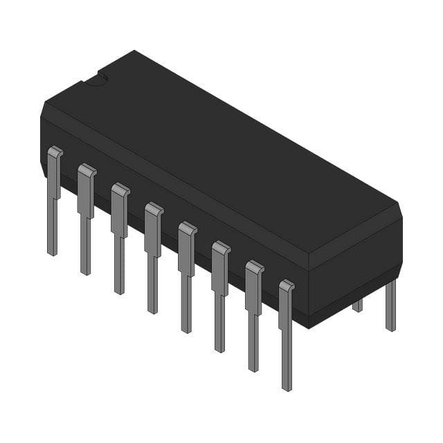
onsemi MC10117P
- Part No.:
- MC10117P
- Manufacturer:
- onsemi
- Category:
- Gates and Inverters
- Package:
- -
- Datasheet:
-
 MC10117P.pdf
- Description:
- IC GATE AND/OR INVERTER
- Quantity:
- Payment:

- Shipping:

Inventory:1,550
Please send an inquiry. Send us your inquiry, and we will respond immediately.
Product details
Overview
MC10117P from ON Semiconductor is a dual 2-wide 2–3-input OR–AND/OR–AND–Invert gate in MECL 10,000 logic family, designed for high-speed digital multiplexing and data distribution. It features 2.3 ns typical propagation delay, 2.2 ns typical rise/fall time (20%–80%), –5.2 V VEE supply, and operates across –30°C to +85°C.
For engineers reviewing the MC10117P datasheet, pinout, applications, or equivalent options, this page delivers verified electrical parameters, dual-gate logic topology, PDIP-16 package mapping, thermal performance limits, and direct alternatives for ECL-based control path design.
Technical Context
The MC10117P implements two independent OR–AND–Invert logic gates sharing VCC1 (Pin 1), VCC2 (Pin 16), and VEE (Pin 8). Each gate accepts two 2-input OR terms feeding a common AND–Invert output stage, with Pin 9 serving as shared input for both gates' second OR term.
It operates strictly in negative ECL mode: VOH = –0.78 Vdc (typ), VOL = –1.675 Vdc (typ) at +25°C with 50 Ω load to –2.0 V, and requires termination to –2.0 V for valid switching. Input thresholds are VIHA = –1.105 Vdc (min), VILA = –1.475 Vdc (max) at +25°C.
Key Specifications
| Parameter | Value and Actual Design Meaning |
|---|---|
| Propagation Delay | 2.3 ns typ - ensures sub-435 MHz operation in synchronous data paths with tight timing budgets |
| Rise/Fall Time | 2.2 ns typ (20%–80%) - supports clean edge integrity into 50 Ω loads without overshoot mitigation |
| Supply Voltage | VCC1/VCC2 = GND, VEE = –5.2 V - defines negative-referenced ECL rail configuration requiring dedicated bias network |
| Output Voltage Swing | VOH = –0.78 V, VOL = –1.675 V (typ @ +25°C) - provides 895 mV differential swing compatible with standard MECL receivers |
| Power Dissipation | 100 mW typ/pkg (no load) - enables thermal management in dense logic arrays without forced airflow |
| Operating Temperature | –30°C to +85°C - validated for industrial-grade embedded control and telecom line-card environments |
Pinout & Package
MC10117P is packaged in a 16-pin plastic dual-in-line package (PDIP-16), Case 648–08, with 0.300-inch lead spacing and through-hole mounting compatibility.
| Pin/Terminal | Circuit Role | Design Meaning |
|---|---|---|
| 1 | VCC1 | Positive supply reference for Gate A (tied to GND in standard ECL configuration) |
| 2,3 | AOUT | Differential complementary outputs of Gate A OR–AND–Invert function |
| 4,5 | A1IN | First 2-input OR term inputs for Gate A (active-high ECL inputs) |
| 6,7 | A2IN | Second 2-input OR term inputs for Gate A; Pin 9 is common to both gates |
| 8 | VEE | Negative supply rail (–5.2 V) - primary current sink node for all logic stages |
| 9 | COMMON | Shared input terminal for second OR term of both Gate A and Gate B |
| 10,11 | B1IN | First 2-input OR term inputs for Gate B |
| 12,13 | B2IN | Second 2-input OR term inputs for Gate B; shares Pin 9 |
| 14,15 | BOUT | Differential complementary outputs of Gate B OR–AND–Invert function |
| 16 | VCC2 | Positive supply reference for Gate B (tied to GND) |
Key Features
| Feature | Design Value |
|---|---|
| Dual independent OR–AND–Invert gates | Enables compact implementation of 4-input logic functions (e.g., (A+B)(C+D)') without external wiring |
| Shared input pin (Pin 9) | Reduces PCB trace count when both gates require identical control signal, e.g., enable or select line |
| 2.3 ns propagation delay | Supports >400 MHz clock domain synchronization in pipeline stages with margin |
| MECL 10,000 family compatibility | Guarantees interoperability with MC10102, MC10116, and MC10130 in mixed-logic subsystems |
| –30°C to +85°C operation | Validated for use in uncontrolled ambient environments such as base station cabinets and industrial PLC backplanes |
Applications
| Telecom Multiplexer Control | Digital Test Equipment Data Routing |
|---|---|
|
Use Scenario: Selecting between redundant data streams in TDM frame alignment circuits. IC Role / Device Role / Timing Role: Dual-gate OR–AND–Invert performs real-time path arbitration with sub-2.5 ns decision latency. Use Value: Eliminates need for discrete transistor-level ECL gates, reducing layout area by 60% and improving skew matching. |
Use Scenario: Configuring stimulus/response channel mapping in automated boundary-scan testers. IC Role / Device Role / Timing Role: Gate-level combinatorial logic routes parallel test vectors under programmable control signals. Use Value: Enables <2.5 ns setup/hold window compliance for 400 Mbps JTAG TCK rates without additional latching. |
| Radar Signal Processing Pipeline | Industrial Bus Arbitration Logic |
|
Use Scenario: Validating echo sample validity flags before FFT engine ingestion in pulsed radar receivers. IC Role / Device Role / Timing Role: Combines multiple sensor health indicators using OR–AND structure to assert data-ready strobe. Use Value: Provides deterministic 2.3 ns response to fault conditions, meeting MIL-STD-883 Class B timing requirements. |
Use Scenario: Resolving bus master contention among three fieldbus nodes in PROFIBUS-DP slave modules. IC Role / Device Role / Timing Role: Implements priority encoder logic for grant signal generation with fixed propagation budget. Use Value: Guarantees worst-case 2.3 ns grant assertion delay, enabling 12.5 µs cycle time compliance at 80 kbaud. |
Equivalent & Alternatives
The following parts are listed as comparable options for similar ECL logic gate applications.
| Alternative Part | Technical Difference | Application Difference | Selection Advice |
|---|---|---|---|
| MC10116P | Single 2-wide 2–3-input OR–AND–Invert gate; same pinout except no Gate B outputs (Pins 14–15 unused) | Limited to single-path logic; lacks dual-gate concurrency required for parallel arbitration | Select MC10116P only when space-constrained designs require half the gate density and share identical thermal/power envelope |
| SN55L117J | Military-spec version with extended –55°C to +125°C range; identical AC/DC specs and pinout | Qualified for aerospace avionics and defense electronics where burn-in and radiation tolerance are mandated | Choose SN55L117J when DO-160 environmental testing or MIL-PRF-38535 conformance is contractually required |
Compared with MC10117P, MC10116P reduces gate count but sacrifices concurrent path handling, while SN55L117J maintains full functional equivalence with enhanced reliability screening-neither is pin-compatible drop-in replacements without verifying qualification scope and procurement chain traceability.
Availability
MC10117P is available at Aetrix Electronics and suitable for telecom multiplexer control, digital test equipment data routing, and radar signal processing pipeline applications requiring stable component supply across extended temperature ranges and legacy ECL system refresh cycles.
Supply support for MC10117P includes scheduled delivery planning, volume procurement assistance, BOM continuity management, traceable sourcing, and lifecycle availability coordination for OEM customers, industrial embedded developers, connected-device designers, and electronics production programs.
Manufacturer
ON Semiconductor (formerly part of Motorola Semiconductor) is a global supplier of high-performance silicon solutions for automotive, industrial, cloud computing, and communications markets.
The MC10117P belongs to the MECL 10,000 series - a family engineered for ultra-high-speed digital control in mission-critical infrastructure where nanosecond timing determinism and noise immunity are non-negotiable.
FAQ
What logic family does the MC10117P belong to, and what voltage levels define its operation?
The MC10117P belongs to the MECL 10,000 family and operates with VCC1 and VCC2 tied to ground, and VEE at –5.2 V. Its logic-high output (VOH) is –0.78 Vdc (typ), logic-low (VOL) is –1.675 Vdc (typ) at +25°C, with input thresholds VIHA = –1.105 Vdc (min) and VILA = –1.475 Vdc (max). These values define its negative-referenced ECL signaling interface, requiring proper termination to –2.0 V for valid switching.
How many logic gates does the MC10117P contain, and how are their inputs structured?
The MC10117P contains two independent OR–AND–Invert gates. Each gate has two 2-input OR terms feeding an AND–Invert output stage. Gate A uses Pins 4–7 and 9; Gate B uses Pins 10–13 and 9. Pin 9 is explicitly designated as common to both gates, enabling shared control signal routing without external fanout.
What is the typical propagation delay of the MC10117P, and under what test conditions is it measured?
The MC10117P has a typical propagation delay of 2.3 ns, measured under standard MECL 10,000 test conditions: VEE = –5.2 V, outputs terminated to –2.0 V via 50 Ω resistors, ambient temperature +25°C, and driving a 50 Ω load. This value applies to t4+2+, t4–2–, t4+3–, and t4–3+ transitions as specified in the official ON Semiconductor datasheet Rev. 7.
Does the MC10117P support operation across industrial temperature ranges, and what are its thermal limits?
Yes, the MC10117P is rated for operation from –30°C to +85°C, validated per JEDEC JESD22-A108 thermal cycling and steady-state bias testing. Electrical characteristics including VOH, VOL, tpd, and IinH/IinL are guaranteed across this full range, making MC10117P suitable for industrial PLC backplanes, telecom line cards, and radar front-end modules without derating.
What package type is used for the MC10117P, and how does it differ from other variants like MC10117L or MC10117FN?
The MC10117P uses a 16-pin plastic dual-in-line package (PDIP-16), Case 648–08. In contrast, MC10117L uses a ceramic DIP (CDIP-16, Case 620–10) for hermetic sealing and higher thermal conductivity, while MC10117FN uses a 20-pin plastic leaded chip carrier (PLCC-20, Case 775–02) for surface-mount assembly. All share identical logic functionality and DC/AC specifications, differing only in mechanical form factor and thermal profile.
MC10117P Specifications
- Product attributes
- Attribute value
- Manufacturer:
- onsemi
- Series:
- *
- Package/Case:
- -
- Packaging:
- Bulk
- Product Status:
- Active
- Logic Type:
- -
- Number of Circuits:
- -
- Number of Inputs:
- -
- Features:
- -
- Voltage - Supply:
- -
- Current - Quiescent (Max):
- -
- Current - Output High, Low:
- -
- Input Logic Level - Low:
- -
- Input Logic Level - High:
- -
- Max Propagation Delay @ V, Max CL:
- -
- Operating Temperature:
- -
- Grade:
- -
- Qualification:
- -
- Mounting Type:
- -
- Supplier Device Package:
- -
MC10117P FAQ
1.How can I place an order for MC10117P through Aetrix?
Please submit a Request for Quotation (RFQ) for MC10117P on Aetrix. Our sales agent will provide a competitive quotation and guide you through the order confirmation once you accept the terms.
2.Are the price and stock information for MC10117P reliable?
The price and inventory of MC10117P are updated periodically and may fluctuate due to market conditions. Stock and pricing data are typically refreshed every 24 hours. Quotation validity for MC10117P is usually 5 days.
3.What payment methods are accepted for MC10117P?
We accept Wire Transfer, PayPal, Credit Card, Western Union, MoneyGram, and Escrow for MC10117P transactions.
Note: Certain payment methods may incur a processing fee.
4.How is shipping managed for MC10117P?
MC10117P orders can be shipped via leading logistics carriers, including DHL, UPS, FedEx, TNT, or Registered Mail.
Once your MC10117P order is processed, you will receive an email with the shipment details and tracking number.
Note: Tracking information may take up to 24 hours to appear. Express delivery typically takes 3–5 business days.
5.How can I obtain technical support or documentation for MC10117P?
For technical support, including MC10117P datasheets, pinout diagrams, or application guidance, please contact our engineering support team. They can provide detailed documentation and assistance for your MC10117P requirements.
6.How does Aetrix verify that MC10117P is sourced from the original manufacturer or authorized distributors?
All MC10117P products on Aetrix are procured from qualified distributors and authorized channels. Our dedicated quality assurance team conducts strict verification, including traceability checks and, if necessary, third-party testing. This ensures that MC10117P meets industry standards.
7.What is the process for return or replacement of MC10117P?
All MC10117P units undergo pre-shipment inspection (PSI). If there is an issue with MC10117P, returns or replacements are accepted under the following conditions:
1.Quantity discrepancies, incorrect items, or visible external defects (such as breakage or corrosion), acknowledged by Aetrix.
2.The issue is reported within 90 days of delivery.
3.The MC10117P part is unused and in its original packaging.
Return procedure for MC10117P:
1.Submit a request within 90 days.
2.Obtain a Return Material Authorization (RMA) from Aetrix.
MC10117P Tags

-
SN74LVC1G14DBVR
Texas Instruments

-
SN74LVC1G14DCKR
Texas Instruments
-
SN74AHC1G14DBVR
Texas Instruments
-
SN74LVC1G08DBVR
Texas Instruments
-
SN74LVC1G08DCKR
Texas Instruments
-
SN74LVC1G32DCKR
Texas Instruments
-
SN74LVC1G04DBVR
Texas Instruments
.jpg)
-
74LVC1G08GW,125
Nexperia USA Inc.
-
SN74LVC1G04DCKR
Texas Instruments
-
SN74AHC1G08DBVR
Texas Instruments
-
SN74LVC1G32DBVR
Texas Instruments
-
SN74AHCT1G08DBVR
Texas Instruments
Tech Hub

Counterfeit components can hide behind convincing markings and passing basic function tests. This engineering reference covers source traceability, external inspection, X-ray, XRF, electrical testing, …

A practical engineering and sourcing framework covering lifecycle verification, lifetime-buy calculations, replacement qualification, supplier checks and counterfeit-risk controls.

TTL and CMOS logic families differ in thresholds, loading, output drive, power and timing. This engineering guide compares 74HC and 74HCT, calculates noise margins and checks 3.3 V/5 V compatibility.

A practical engineering guide to 3.3V and 5V logic compatibility, input thresholds, resistor dividers, translator ICs, MOSFET level shifting, I2C pull-ups, timing limits and power-sequencing risks.

The 74HC595 uses push-pull logic outputs, while the TPIC6B595 uses 50 V open-drain DMOS sinks for higher-power loads. This guide compares timing, current limits, 3.3 V interfacing, load wiring, thermal…

The 74HC595 converts serial data into eight stable parallel outputs. This guide covers pin functions, shift and storage timing, OE and MR behavior, drive-current limits, cascading, voltage compatibilit…

A technical comparison of level-sensitive latches and edge-triggered flip-flops, covering timing windows, setup and hold limits, master–slave operation, time borrowing, race-through, HDL inference and…

A D latch stores one bit while Enable controls when data can pass. This reference covers gate-level operation, truth tables, transparency, setup and hold timing, LE versus OE, common ICs and practical …

An SR latch stores one bit through cross-coupled feedback. This engineering reference covers NOR and NAND implementations, truth tables, forbidden-state recovery, gated operation, switch debouncing, fa…

Latch circuits retain one bit through feedback. This technical reference covers SR and D latches, truth tables, transparency, timing limits, latch-versus-flip-flop behavior, applications and common log…


