
 My Inquiry
 My Account


NXP Semiconductors MC10XS3412CPNA
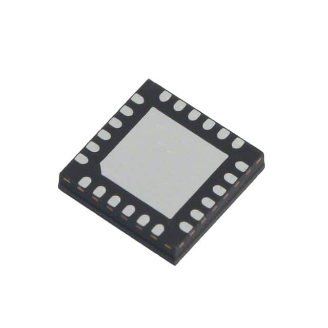
- Part No.:
- MC10XS3412CPNA
- Manufacturer:
- NXP Semiconductors
- Package:
- 24-PowerQFN
- Datasheet:
-
 MC10XS3412CPNA.pdf
- Description:
- IC PWR SWITCH N-CHAN 1:1 24PQFN
- Quantity:
- Payment:

- Shipping:

Inventory:1,583
Please send an inquiry. Send us your inquiry, and we will respond immediately.
Product details
Overview
MC10XS3412CPNA from NXP Semiconductors is a quad high-side switch IC designed for automotive lighting control, featuring dual 10 mΩ and dual 12 mΩ RDS(on) MOSFETs at 25 °C, 6.0–20 V operating voltage, 8 MHz SPI interface, and programmable fault current trip levels. It drives four independent 55/28 W bulbs, Xenon modules, or LEDs in low-voltage vehicle systems.
For engineers reviewing the MC10XS3412CPNA datasheet, MC10XS3412CPNA pinout, MC10XS3412CPNA application, or MC10XS3412CPNA equivalent, key selection considerations include its 24-pin PQFN package, selectable slew-rate outputs for EMC compliance, Fail-safe mode operation during MCU failure, analog current feedback with configurable ratio, and PWM control via parallel inputs or SPI-managed internal oscillator.
Technical Context
The MC10XS3412CPNA integrates four protected high-side power switches with independent overcurrent, short-circuit, and overtemperature protection, each supporting programmable fault blanking (5.0 μs) and shutdown delay (7.0 μs). Its SPI-controlled architecture enables daisy-chain configuration and real-time status reporting.
Functional operation includes dual-mode control-direct parallel input (IN0–IN3) for simple ON/OFF or PWM timing, and full-featured 16-bit SPI for diagnostics, current sensing calibration, lamp inrush management, and Fail-safe activation via FSI. The device uses an internal regulator and charge pump to sustain gate drive across the 4.0–28 V extended VPWR range.
Key Specifications
| Parameter | Value and Actual Design Meaning |
|---|---|
| RDS(on) HS0/HS1 | 10 mΩ @ 5 A, 25 °C - enables efficient 55 W bulb driving with <100 mW conduction loss |
| RDS(on) HS2/HS3 | 12 mΩ @ 5 A, 25 °C - optimized for 28 W loads with balanced thermal performance |
| Supply range VPWR | 6.0–20 V operational / 4.0–28 V extended - supports cold-crank and load-dump conditions in 12 V automotive systems |
| SPI interface | 8.0 MHz, 3.3 V/5.0 V compatible, daisy-chain capable - allows multi-device control with minimal MCU GPIO usage |
| Sleep current | <5.0 μA @ 12 V - meets automotive module quiescent current requirements for always-on nodes |
| Fault detection | Programmable trip level & duration, time-limited autoretry - prevents nuisance shutdown during lamp inrush |
| Current sense | Configurable CSNS ratio (1/4350 to 1/53000), ±12% accuracy - enables precise closed-loop LED or filament current monitoring |
Pinout & Package
MC10XS3412CPNA is housed in a 24-pin PQFN package (98ARL10596D / 98ASA00426D), Pb-free, with exposed thermal pad. Pin pitch is 0.5 mm; package footprint is 5 mm × 5 mm × 0.85 mm (max height).
| Pin/Terminal | Circuit Role | Design Meaning |
|---|---|---|
| HS0, HS1, HS2, HS3 | High-side power outputs | Protected 10 mΩ (HS0/HS1) or 12 mΩ (HS2/HS3) switched VPWR connections to loads; support PWM, open-load, and short-to-battery detection |
| IN0–IN3 | Direct control inputs | Parallel TTL/CMOS inputs enabling immediate output state override or external clock injection for PWM generation |
| CSNS | Analog current/temperature monitor | Single pin multiplexed for proportional current feedback (IHS) or GND flag temperature sensing; ratio selected via SPI |
| FS | Fault status output | Open-drain active-low signal indicating overcurrent, overtemperature, or undervoltage fault; requires external VDD pull-up |
| FSI | Fail-safe enable input | Active-high input that activates hardware-based Fail-safe mode when MCU fails; internal pull-up to ~3.0 V |
| WAKE, RST, CS, SCLK, SI, SO | SPI and system control | Standard 3.3/5 V SPI interface plus wake/reset logic; supports daisy-chaining via SI/SO; all inputs have defined VIH/VIL and internal biasing |
| VPWR, VDD, GND | Power domains | VPWR powers high-side drivers and protection circuitry (4–28 V); VDD powers digital core (3–5.5 V); three GND pins ensure low-impedance return path |
Key Features
| Feature | Design Value |
|---|---|
| Selectable output slew rate | Three programmable rise/fall rates (0.07–1.2 V/μs) per channel to optimize EMI vs. switching speed trade-off |
| Fail-safe mode | Hardware-enforced output state retention (ON/OFF per ON[0:3] register) upon MCU communication loss or reset failure |
| Smart overcurrent shutdown | Configurable trip thresholds and time steps (e.g., 1.1–73.2 ms for 28 W bit = 0) prevent false trips during lamp cold-start |
| Open-load detection | Differentiated OFF-state (30–100 μA sourcing) and ON-state (100–600 mA sinking) thresholds for bulbs and LEDs |
| Calibratable internal oscillator | Enables standalone PWM generation without external clock; frequency adjustable via SPI for dimming consistency |
Applications
| Automotive Front Lighting | Adaptive Driving Beam (ADB) Modules |
|---|---|
Use Scenario: Controlling individual LED segments in matrix headlamps for dynamic beam shaping and glare-free high-beam operation. IC Role / Device Role / Timing Role: Quad high-side driver providing independent, PWM-modulated current control to four LED sub-arrays with real-time current feedback. Use Value: Enables precise per-segment brightness control (via CSNS feedback) and fast fault response (<10 μs blanking) to maintain beam integrity during transients. | Use Scenario: Powering and protecting multiple Xenon or halogen position lamps in adaptive cornering light systems. IC Role / Device Role / Timing Role: High-side switch managing inrush-limited turn-on of 55/28 W filaments with programmable lamp-cooling timing (6.4–232 ms). Use Value: Prevents filament shock failure via controlled slew rate and extends lamp life using calibrated overcurrent trip profiles. |
| Commercial Vehicle Rear Lighting | Electronic Control Unit (ECU) Subsystem |
Use Scenario: Replacing electromechanical relays in trailer connector modules for brake, turn, and tail lights. IC Role / Device Role / Timing Role: Solid-state replacement delivering diagnostic-ready switching with open-load and short-to-battery detection on all four channels. Use Value: Eliminates relay wear-out, reduces PCB space by >70%, and provides CAN-agnostic fault reporting via FS pin and SPI registers. | Use Scenario: Integrating into body control modules (BCMs) requiring fail-operational lighting control during MCU brownout or crash events. IC Role / Device Role / Timing Role: Safety-critical high-side driver entering hardware-defined Fail-safe mode when FSI is asserted or watchdog times out (217–400 ms). Use Value: Maintains critical lighting functions (e.g., hazard flashers) without software intervention, meeting ISO 26262 ASIL-B functional safety requirements. |
Equivalent & Alternatives
The following parts are listed as comparable options for similar high-side switch applications.
| Alternative Part | Technical Difference | Application Difference | Selection Advice |
|---|---|---|---|
| MC10XS3412JHFK | Identical electrical specs and pinout; differs only in temperature grade (–40 to 125 °C vs. –40 to 150 °C junction max for CHFK) | Targeted at under-hood applications with higher ambient thermal stress; same PCB layout and firmware compatibility | Select MC10XS3412JHFK for cost-sensitive cabin modules where junction temperature remains below 150 °C |
| MC10XS3412CHFK | Same die, identical functionality, and 24-pin PQFN package; qualified for higher junction temperature (150 °C vs. 125 °C ambient for JHFK) | Required for engine bay or headlamp ECU deployments where sustained 125 °C ambient is expected | Choose MC10XS3412CHFK when operating ambient exceeds 105 °C or thermal margin must cover worst-case junction rise |
Compared with MC10XS3412JHFK and MC10XS3412CHFK, the MC10XS3412CPNA shares identical silicon, pinout, and feature set - differing only in tape-and-reel packaging (PNA suffix denotes 2,500-unit reel); all three support the same SPI register map, protection algorithms, and diagnostic capabilities.
Availability
MC10XS3412CPNA is available at Aetrix Electronics and suitable for automotive front lighting, adaptive driving beam modules, commercial vehicle rear lighting, and electronic control unit subsystems requiring stable component supply, long-term lifecycle support, and AEC-Q100-compliant sourcing.
Supply support for MC10XS3412CPNA includes scheduled delivery planning, volume procurement assistance, BOM continuity management, traceable sourcing, and lifecycle availability coordination for OEM customers, industrial embedded developers, connected-device designers, and electronics production programs.
Manufacturer
NXP Semiconductors is a global semiconductor leader focused on secure connectivity solutions for automotive, industrial, and IoT applications.
The MC10XS3412CPNA belongs to NXP's automotive high-side switch product line, engineered specifically for intelligent, diagnostic-capable lighting control in 12 V vehicle architectures with stringent EMC and functional safety requirements.
FAQ
What is the maximum continuous output current rating for MC10XS3412CPNA?
The MC10XS3412CPNA supports up to 6 A continuous output current per channel (HS0–HS3), provided the maximum junction temperature of 150 °C is not exceeded. Actual current capability depends on PCB thermal design - with RθJA = 30 °C/W, sustained 6 A operation requires careful heatsinking or derating above 85 °C ambient. The device includes thermal shutdown at 155–195 °C to protect against overload.
Does MC10XS3412CPNA support both SPI and direct parallel control simultaneously?
Yes, MC10XS3412CPNA supports concurrent SPI and direct parallel control: IN0–IN3 pins provide immediate hardware-level ON/OFF or PWM timing override, while the SPI interface manages configuration, diagnostics, and fine-grained parameter tuning. When both are active, INx inputs take precedence for output state, ensuring deterministic behavior during MCU resets or communication loss.
How does the Fail-safe mode function in MC10XS3412CPNA?
In MC10XS3412CPNA, Fail-safe mode is activated when the FSI pin is driven high or after watchdog timeout (217–400 ms). Once engaged, the device retains the last commanded output states (ON[0:3]) using internal latches, independent of SPI or INx signals. This ensures critical lighting functions remain operational even if the host MCU fails, satisfying ASIL-B functional safety requirements for automotive systems.
What are the supported current sense ratios for CSNS on MC10XS3412CPNA?
MC10XS3412CPNA offers four programmable CSNS current sense ratios via SPI: 1/4350 and 1/26500 (when 28 W bit = 1), or 1/8700 and 1/53000 (when 28 W bit = 0). These ratios allow precise scaling of sensed output current (IHS) to a 0–VDD analog voltage on CSNS, with ±12% accuracy at 5 A and temperature drift of 0.04 %/°C for CSR0 configurations.
Can MC10XS3412CPNA drive LED loads with constant-current regulation?
MC10XS3412CPNA does not provide closed-loop constant-current regulation itself but enables it via external feedback: its CSNS pin delivers an analog voltage proportional to output current, which can be fed into an MCU's ADC for software-based current control. Combined with programmable PWM timing and slew rate, this architecture supports accurate LED dimming and thermal derating - verified in NXP reference designs for automotive LED headlamps.
MC10XS3412CPNA Specifications
- Product attributes
- Attribute value
- Manufacturer:
- NXP Semiconductors
- Package/Case:
- 24-PowerQFN
- Series:
- -
- Packaging:
- Tray
- Product Status:
- Obsolete
- Switch Type:
- General Purpose
- Number of Outputs:
- 4
- Ratio - Input:Output:
- 1:1
- Output Configuration:
- High Side
- Output Type:
- N-Channel
- Interface:
- SPI
- Voltage - Load:
- 6V ~ 20V
- Voltage - Supply (Vcc/Vdd):
- 3V ~ 5.5V
- Current - Output (Max):
- -
- Rds On (Typ):
- 10mOhm, 12mOhm
- Input Type:
- -
- Features:
- Internal PWM, Slew Rate Controlled, Watchdog Timer
- Fault Protection:
- Current Limiting (Fixed), Open Load Detect, Over Temperature, Over Voltage
- Operating Temperature:
- -40°C ~ 150°C (TJ)
- Grade:
- -
- Qualification:
- -
- Mounting Type:
- Surface Mount
- Supplier Device Package:
- 24-PQFN (12x12)
MC10XS3412CPNA FAQ
1.How can I place an order for MC10XS3412CPNA through Aetrix?
Please submit a Request for Quotation (RFQ) for MC10XS3412CPNA on Aetrix. Our sales agent will provide a competitive quotation and guide you through the order confirmation once you accept the terms.
2.Are the price and stock information for MC10XS3412CPNA reliable?
The price and inventory of MC10XS3412CPNA are updated periodically and may fluctuate due to market conditions. Stock and pricing data are typically refreshed every 24 hours. Quotation validity for MC10XS3412CPNA is usually 5 days.
3.What payment methods are accepted for MC10XS3412CPNA?
We accept Wire Transfer, PayPal, Credit Card, Western Union, MoneyGram, and Escrow for MC10XS3412CPNA transactions.
Note: Certain payment methods may incur a processing fee.
4.How is shipping managed for MC10XS3412CPNA?
MC10XS3412CPNA orders can be shipped via leading logistics carriers, including DHL, UPS, FedEx, TNT, or Registered Mail.
Once your MC10XS3412CPNA order is processed, you will receive an email with the shipment details and tracking number.
Note: Tracking information may take up to 24 hours to appear. Express delivery typically takes 3–5 business days.
5.How can I obtain technical support or documentation for MC10XS3412CPNA?
For technical support, including MC10XS3412CPNA datasheets, pinout diagrams, or application guidance, please contact our engineering support team. They can provide detailed documentation and assistance for your MC10XS3412CPNA requirements.
6.How does Aetrix verify that MC10XS3412CPNA is sourced from the original manufacturer or authorized distributors?
All MC10XS3412CPNA products on Aetrix are procured from qualified distributors and authorized channels. Our dedicated quality assurance team conducts strict verification, including traceability checks and, if necessary, third-party testing. This ensures that MC10XS3412CPNA meets industry standards.
7.What is the process for return or replacement of MC10XS3412CPNA?
All MC10XS3412CPNA units undergo pre-shipment inspection (PSI). If there is an issue with MC10XS3412CPNA, returns or replacements are accepted under the following conditions:
1.Quantity discrepancies, incorrect items, or visible external defects (such as breakage or corrosion), acknowledged by Aetrix.
2.The issue is reported within 90 days of delivery.
3.The MC10XS3412CPNA part is unused and in its original packaging.
Return procedure for MC10XS3412CPNA:
1.Submit a request within 90 days.
2.Obtain a Return Material Authorization (RMA) from Aetrix.
MC10XS3412CPNA Tags

-
TPS22919DCKR
Texas Instruments

-
MIC2091-1YM5-TR
Microchip Technology

-
MIC2090-1YM5-TR
Microchip Technology

-
TPS22995RZFR
Texas Instruments

-
TPS22975DSGR
Texas Instruments

-
SIP32510DT-T1-GE3
Vishay Siliconix

-
ULN2003D1013TR
STMicroelectronics

-
MIC2005A-1YM5-TR
Microchip Technology

-
MIC2005A-1YM6-TR
Microchip Technology

-
TPS22916BYFPR
Texas Instruments

-
TPS22917DBVR
Texas Instruments

-
ULN2003APWR
Texas Instruments
Tech Hub

A practical engineering guide to 3.3V and 5V logic compatibility, input thresholds, resistor dividers, translator ICs, MOSFET level shifting, I2C pull-ups, timing limits and power-sequencing risks.

The 74HC595 uses push-pull logic outputs, while the TPIC6B595 uses 50 V open-drain DMOS sinks for higher-power loads. This guide compares timing, current limits, 3.3 V interfacing, load wiring, thermal…

The 74HC595 converts serial data into eight stable parallel outputs. This guide covers pin functions, shift and storage timing, OE and MR behavior, drive-current limits, cascading, voltage compatibilit…

A technical comparison of level-sensitive latches and edge-triggered flip-flops, covering timing windows, setup and hold limits, master–slave operation, time borrowing, race-through, HDL inference and…

A D latch stores one bit while Enable controls when data can pass. This reference covers gate-level operation, truth tables, transparency, setup and hold timing, LE versus OE, common ICs and practical …

An SR latch stores one bit through cross-coupled feedback. This engineering reference covers NOR and NAND implementations, truth tables, forbidden-state recovery, gated operation, switch debouncing, fa…

Latch circuits retain one bit through feedback. This technical reference covers SR and D latches, truth tables, transparency, timing limits, latch-versus-flip-flop behavior, applications and common log…

An engineering guide to LED driver operation, constant-current and constant-voltage outputs, linear and switching topologies, dimming, IC selection, calculations, replacement compatibility, and fault c…

Operational amplifier guide covering op amp basics, feedback, ideal vs real op amps, common configurations, buffer circuits, offset, bias current, gain-bandwidth, slew rate, rail-to-rail limits and sel…

Jumper cables guide covering safe connection order, red and black clamp placement, final ground connection, cable gauge, length, clamp quality, copper vs CCA cables, jump starter comparison and battery…


