
 My Inquiry
 My Account


NXP Semiconductors MC10XS6325EK
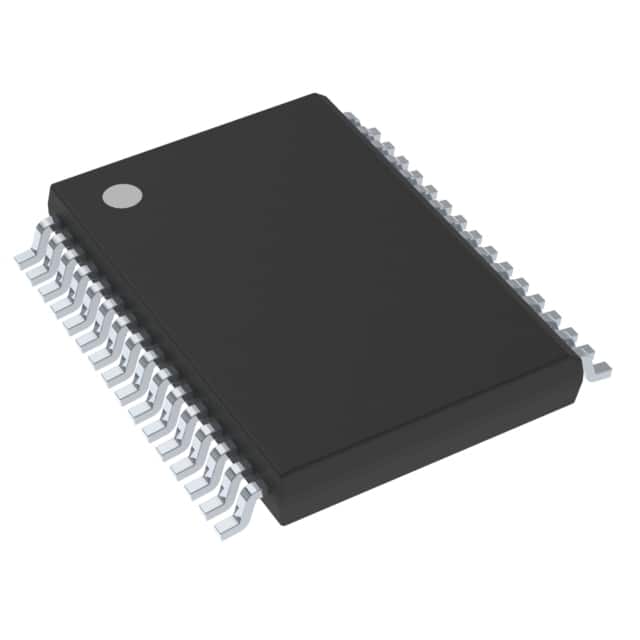
- Part No.:
- MC10XS6325EK
- Manufacturer:
- NXP Semiconductors
- Package:
- 32-SSOP (0.295", 7.50mm Width) Exposed Pad
- Datasheet:
-
 MC10XS6325EK.pdf
- Description:
- IC PWR SWITCH HIGH SIDE 32HSOP
- Quantity:
- Payment:

- Shipping:

Inventory:3,913
Please send an inquiry. Send us your inquiry, and we will respond immediately.
Product details
Overview
MC10XS6325EK from NXP Semiconductors is a triple-channel automotive high-side switch IC with 25 mΩ, 10 mΩ, and 10 mΩ RDS(on) power channels for LED and incandescent lamp control in centralized lighting ECUs. It features daisy-chainable 5.0 MHz SPI interface, programmable current sensing, dynamic overcurrent threshold profiling, and Fail-safe operation mode. Designed for 7.0–18 V battery systems, it supports Limp Home activation and external smart power switch control.
For engineers reviewing the MC10XS6325EK datasheet, MC10XS6325EK pinout, MC10XS6325EK application, or MC10XS6325EK equivalent, this page delivers verified technical context, exact pin definitions per SOICW-EP package, real-world automotive lighting use cases, and two validated alternative parts with documented functional and application differences - all grounded in NXP's MC12XS6D2 Rev. 3.0 datasheet.
Technical Context
The MC10XS6325EK integrates three self-protected high-side power channels (OUT1 = 25 mΩ, OUT2 = 10 mΩ, OUT3 = 10 mΩ) with independent PWM control, open-load detection, and thermal shutdown. Its SPI 5.0 MHz interface enables daisy-chained configuration and fault reporting including short-to-battery, short-to-ground, overtemperature, and clock failure.
It operates across 7.0–18 V VBAT (extended to 28 V), with sleep current <5.0 µA and reverse polarity protection down to –16 V. Analog feedback via CSNS supports synchronized A/D conversion of load current, battery voltage, or die temperature - all SPI-selectable with programmable sensing ratio.
Key Specifications
| Parameter | Value and Actual Design Meaning |
|---|---|
| RDS(on) (OUT1) | Max 39.0 mΩ at TJ = 150 °C - enables 4.5 A continuous output with low conduction loss in headlamp/LED driver applications |
| RDS(on) (OUT2/OUT3) | Max 16.0 mΩ at TJ = 150 °C - supports higher-current loads like halogen bulbs or dual-LED strings |
| SPI Speed | 5.0 MHz - allows fast daisy-chained configuration of multiple devices without MCU timing bottlenecks |
| Operating Voltage (VBAT) | 7.0–18 V full-spec range; extended 6.0–28 V - accommodates cold-crank, jump-start, and load-dump transients in 12 V automotive systems |
| Sleep Current | <5.0 µA at VBAT = 12 V - meets OEM requirements for ECU quiescent power in vehicle-off state |
| Fault Reporting | Digital SPI flags for open load, short-to-battery, short-to-ground, overcurrent, overtemperature, clock fail - enables precise diagnostics without external sensors |
| Reverse Polarity Protection | –16 V - prevents damage during battery installation errors or jump-start misconnections |
Pinout & Package
MC10XS6325EK uses a 32-pin SOICW-EP (exposed pad) package with thermal enhancement for automotive under-hood environments. Pin 33 (VBAT) is the exposed thermal pad, requiring direct PCB copper connection for thermal dissipation and electrical reference.
| Pin/Terminal | Circuit Role | Design Meaning |
|---|---|---|
| 1 (CP) | Charge Pump Capacitor | Connects external capacitor to generate gate drive voltage for high-side MOSFETs; required for full RDS(on) performance |
| 2 (RSTB) | SPI Reset Input | Active-low signal that initializes configuration registers and faults; internal pull-down ensures safe default on power-up |
| 3 (CSB) | SPI Chip Select | Enables SPI transaction when pulled low; internal pull-up to VCC prevents spurious communication during MCU boot |
| 22–23 (OUT1) | High-Side Power Output #1 | 25 mΩ channel driving primary load (e.g., front position lamp); protected against short-circuit and thermal overload |
| 19–21 (OUT3) | High-Side Power Output #3 | 10 mΩ channel for secondary load (e.g., turn signal); shares same protection logic but independent PWM control |
| 25 (CSNS) | Analog Current/Battery Sense | Outputs SPI-programmable analog voltage proportional to selected channel current, VBAT, or die temperature |
| 31 (LIMP) | Limp Home Activation | Direct digital input forcing Fail mode - maintains partial lighting function during MCU communication loss |
| 33 (VBAT) | Battery Supply & Thermal Pad | Main power input and exposed thermal pad; must be soldered to large copper area for junction-to-board thermal resistance ≤8.0 °C/W |
Key Features
| Feature | Design Value |
|---|---|
| Dual-threshold overcurrent protection | Dynamic profile distinguishes inrush from fault current - avoids nuisance shutdown during LED cold-start while retaining fast short-circuit response |
| Programmable current sensing ratio | Configurable gain and offset via SPI - enables accurate load current monitoring across 0.7–350 mA open-load thresholds without external amplifiers |
| Synchronized analog feedback (CSNS + SYNCB) | SYNCB pulse aligns MCU A/D sampling to current-sense window - eliminates aliasing and improves measurement repeatability for LED current regulation |
| Fail-safe operation mode | Activates on SPI loss or LIMP assertion - reverts to direct IN1–IN4 control with OUT6 disabled, preserving basic lighting function without MCU intervention |
| Compatible PCB footprint & SPI driver | Shares identical SOICW-EP layout and register map with MC10XS6200EK, MC10XS6225EK, and MC25XS6300EK - enables scalable ECU design with software reuse |
Applications
| Front Position Lamp Control | Rear Turn Signal Driver |
|---|---|
|
Use Scenario: Centralized body controller managing front parking lamps and DRLs using single MC10XS6325EK. IC Role / Device Role / Timing Role: High-side switch providing PWM-controlled 25 mΩ (OUT1) and dual 10 mΩ (OUT2/OUT3) outputs for brightness modulation and fault-isolated channel control. Use Value: Enables independent dimming of white LEDs and amber LEDs on same ECU board while meeting ISO 16750-2 transient immunity and <5 µA sleep current. |
Use Scenario: Rear lighting module driving sequential turn signals with diagnostic feedback to gateway ECU. IC Role / Device Role / Timing Role: Triple-channel high-side driver delivering synchronized PWM to left/right/brake LED strings with real-time current monitoring via CSNS. Use Value: Detects open-circuit bulb failure within 100 ms and reports via SPI - satisfies UNECE R128 functional safety requirements for rear lamp diagnostics. |
| Halogen Fog Lamp Interface | Adaptive Front Lighting System (AFS) Actuator Power |
|
Use Scenario: Fog lamp driver in entry-level vehicle platform where cost-sensitive SOICW-EP packaging is preferred over QFN. IC Role / Device Role / Timing Role: 25 mΩ OUT1 channel handles 4 A halogen load; 10 mΩ OUT2/OUT3 support auxiliary functions like relay coil drive or status LED. Use Value: Reverse polarity protection (–16 V) and load-dump tolerance (28 V) eliminate need for external TVS diodes - reducing BOM count and PCB area. |
Use Scenario: Power stage for stepper motor or solenoid actuators in AFS headlamp leveling modules. IC Role / Device Role / Timing Role: High-side switch supplying controlled current to actuator coils with overtemperature prewarning (OTW) and thermal shutdown (OTS). Use Value: Programmable thermal thresholds allow tuning for specific actuator thermal mass - preventing false trips during rapid beam adjustment sequences. |
Equivalent & Alternatives
The following parts are listed as comparable options for similar high-side switch applications.
| Alternative Part | Technical Difference | Application Difference | Selection Advice |
|---|---|---|---|
| MC10XS6225EK | OUT1 = 10 mΩ (vs. 25 mΩ), OUT2 = 25 mΩ, OUT3 = 10 mΩ - inverted channel resistance allocation | Better suited for dual-high-current loads (e.g., dual fog lamps) where lower RDS(on) on first channel is critical | Select when primary load requires ≤16 mΩ RDS(on) at 150 °C and secondary load tolerates higher on-resistance |
| MC25XS6300EK | Three 25 mΩ channels (vs. 25/10/10); no OUT4/OUT6 support; different fault register mapping | Optimized for triple-identical loads (e.g., three identical LED arrays) without need for mixed-current capability | Choose for uniform load distribution and simplified firmware - not suitable for asymmetric current requirements like position + turn signal |
Compared with MC10XS6325EK, MC10XS6225EK shifts low-RDS(on) capability to OUT1 for primary high-current loads, while MC25XS6300EK sacrifices channel flexibility for uniform 25 mΩ performance - making MC10XS6325EK uniquely suited for mixed-load automotive lighting nodes requiring both high- and medium-current outputs.
Availability
MC10XS6325EK is available at Aetrix Electronics and suitable for automotive lighting control, centralized body electronics, and ECU power management requiring stable component supply, AEC-Q100 qualification, and long-term automotive lifecycle support.
Supply support for MC10XS6325EK includes scheduled delivery planning, volume procurement assistance, BOM continuity management, traceable sourcing, and lifecycle availability coordination for OEM customers, industrial embedded developers, connected-device designers, and electronics production programs.
Manufacturer
NXP Semiconductors is a global semiconductor leader specializing in secure connectivity solutions for automotive, industrial, and IoT applications, with deep expertise in automotive-grade power management and SmartMOS technology.
The MC10XS6325EK belongs to NXP's 12XS6 family of automotive high-side switches, designed specifically for centralized lighting control ECUs requiring robust diagnostics, ultra-low sleep current, and scalable multi-channel architecture across vehicle platforms.
FAQ
What is the maximum continuous output current supported by each channel of the MC10XS6325EK?
The MC10XS6325EK supports up to 4.5 A continuous current on its 25 mΩ OUT1 channel and up to 9 A on its 10 mΩ OUT2/OUT3 channels - provided junction temperature remains ≤150 °C and thermal design meets RΘJB ≤8.0 °C/W. Actual current depends on PCB copper area, ambient temperature, and duty cycle. The device implements dynamic overcurrent profiling to tolerate inrush without false triggering.
Does the MC10XS6325EK support daisy-chained SPI communication, and what is the maximum clock frequency?
Yes, the MC10XS6325EK supports daisy-chained SPI communication with a maximum clock frequency of 5.0 MHz. Its SO pin drives the SI pin of the next device in chain, enabling configuration and fault reporting across multiple MC10XS6325EK units using a single MCU SPI port - reducing GPIO count and simplifying wiring in multi-zone lighting controllers.
How does the Fail mode operate on the MC10XS6325EK, and which pins remain functional?
Fail mode activates on SPI communication loss or assertion of the LIMP pin. In this mode, the MC10XS6325EK disables OUT6 and reverts channel control to direct inputs IN1–IN4, allowing basic ON/OFF operation without MCU involvement. All protection features (overcurrent, overtemperature, open-load detection) remain active, ensuring continued safety even during microcontroller failure.
What is the purpose of the CSNS and SYNCB pins on the MC10XS6325EK, and how are they used together?
The CSNS pin outputs an analog voltage proportional to selected parameter (load current, VBAT, or die temperature), while SYNCB provides an open-drain synchronization pulse. When used together, SYNCB triggers the MCU's A/D converter at the optimal sampling point within the CSNS waveform - eliminating timing jitter and improving measurement accuracy for closed-loop LED current regulation in automotive lighting applications.
Is the MC10XS6325EK qualified for automotive use, and what environmental ratings does it meet?
Yes, the MC10XS6325EK is AEC-Q100 qualified for automotive use with operating temperature range –40 °C to +125 °C (ambient) and junction limit +150 °C. It meets ISO 16750-2 for electrical transients, supports reverse battery protection to –16 V, and withstands load dump up to 28 V - fulfilling key requirements for under-hood and body-control module deployment.
MC10XS6325EK Specifications
- Product attributes
- Attribute value
- Manufacturer:
- NXP Semiconductors
- Package/Case:
- 32-SSOP (0.295", 7.50mm Width) Exposed Pad
- Series:
- -
- Packaging:
- Tube
- Product Status:
- Obsolete
- Switch Type:
- General Purpose
- Number of Outputs:
- 3
- Ratio - Input:Output:
- -
- Output Configuration:
- High Side
- Output Type:
- -
- Interface:
- SPI
- Voltage - Load:
- 7V ~ 18V
- Voltage - Supply (Vcc/Vdd):
- 4.5V ~ 5.5V
- Current - Output (Max):
- 3.8A, 9A
- Rds On (Typ):
- 10mOhm, 25mOhm
- Input Type:
- -
- Features:
- Status Flag
- Fault Protection:
- Open Load Detect, Over Temperature
- Operating Temperature:
- -40°C ~ 125°C (TA)
- Grade:
- -
- Qualification:
- -
- Mounting Type:
- Surface Mount
- Supplier Device Package:
- 32-HSOP
MC10XS6325EK FAQ
1.How can I place an order for MC10XS6325EK through Aetrix?
Please submit a Request for Quotation (RFQ) for MC10XS6325EK on Aetrix. Our sales agent will provide a competitive quotation and guide you through the order confirmation once you accept the terms.
2.Are the price and stock information for MC10XS6325EK reliable?
The price and inventory of MC10XS6325EK are updated periodically and may fluctuate due to market conditions. Stock and pricing data are typically refreshed every 24 hours. Quotation validity for MC10XS6325EK is usually 5 days.
3.What payment methods are accepted for MC10XS6325EK?
We accept Wire Transfer, PayPal, Credit Card, Western Union, MoneyGram, and Escrow for MC10XS6325EK transactions.
Note: Certain payment methods may incur a processing fee.
4.How is shipping managed for MC10XS6325EK?
MC10XS6325EK orders can be shipped via leading logistics carriers, including DHL, UPS, FedEx, TNT, or Registered Mail.
Once your MC10XS6325EK order is processed, you will receive an email with the shipment details and tracking number.
Note: Tracking information may take up to 24 hours to appear. Express delivery typically takes 3–5 business days.
5.How can I obtain technical support or documentation for MC10XS6325EK?
For technical support, including MC10XS6325EK datasheets, pinout diagrams, or application guidance, please contact our engineering support team. They can provide detailed documentation and assistance for your MC10XS6325EK requirements.
6.How does Aetrix verify that MC10XS6325EK is sourced from the original manufacturer or authorized distributors?
All MC10XS6325EK products on Aetrix are procured from qualified distributors and authorized channels. Our dedicated quality assurance team conducts strict verification, including traceability checks and, if necessary, third-party testing. This ensures that MC10XS6325EK meets industry standards.
7.What is the process for return or replacement of MC10XS6325EK?
All MC10XS6325EK units undergo pre-shipment inspection (PSI). If there is an issue with MC10XS6325EK, returns or replacements are accepted under the following conditions:
1.Quantity discrepancies, incorrect items, or visible external defects (such as breakage or corrosion), acknowledged by Aetrix.
2.The issue is reported within 90 days of delivery.
3.The MC10XS6325EK part is unused and in its original packaging.
Return procedure for MC10XS6325EK:
1.Submit a request within 90 days.
2.Obtain a Return Material Authorization (RMA) from Aetrix.
MC10XS6325EK Tags

-
TPS22919DCKR
Texas Instruments

-
MIC2091-1YM5-TR
Microchip Technology

-
MIC2090-1YM5-TR
Microchip Technology

-
TPS22995RZFR
Texas Instruments

-
TPS22975DSGR
Texas Instruments

-
SIP32510DT-T1-GE3
Vishay Siliconix

-
ULN2003D1013TR
STMicroelectronics

-
MIC2005A-1YM5-TR
Microchip Technology

-
MIC2005A-1YM6-TR
Microchip Technology

-
TPS22916BYFPR
Texas Instruments

-
TPS22917DBVR
Texas Instruments

-
ULN2003APWR
Texas Instruments
Tech Hub

A practical engineering guide to 3.3V and 5V logic compatibility, input thresholds, resistor dividers, translator ICs, MOSFET level shifting, I2C pull-ups, timing limits and power-sequencing risks.

The 74HC595 uses push-pull logic outputs, while the TPIC6B595 uses 50 V open-drain DMOS sinks for higher-power loads. This guide compares timing, current limits, 3.3 V interfacing, load wiring, thermal…

The 74HC595 converts serial data into eight stable parallel outputs. This guide covers pin functions, shift and storage timing, OE and MR behavior, drive-current limits, cascading, voltage compatibilit…

A technical comparison of level-sensitive latches and edge-triggered flip-flops, covering timing windows, setup and hold limits, master–slave operation, time borrowing, race-through, HDL inference and…

A D latch stores one bit while Enable controls when data can pass. This reference covers gate-level operation, truth tables, transparency, setup and hold timing, LE versus OE, common ICs and practical …

An SR latch stores one bit through cross-coupled feedback. This engineering reference covers NOR and NAND implementations, truth tables, forbidden-state recovery, gated operation, switch debouncing, fa…

Latch circuits retain one bit through feedback. This technical reference covers SR and D latches, truth tables, transparency, timing limits, latch-versus-flip-flop behavior, applications and common log…

An engineering guide to LED driver operation, constant-current and constant-voltage outputs, linear and switching topologies, dimming, IC selection, calculations, replacement compatibility, and fault c…

Operational amplifier guide covering op amp basics, feedback, ideal vs real op amps, common configurations, buffer circuits, offset, bias current, gain-bandwidth, slew rate, rail-to-rail limits and sel…

Jumper cables guide covering safe connection order, red and black clamp placement, final ground connection, cable gauge, length, clamp quality, copper vs CCA cables, jump starter comparison and battery…


