
 My Inquiry
 My Account


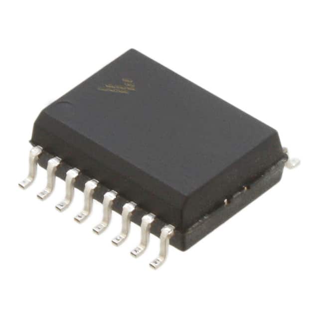
NXP Semiconductors MC145028DWR2
- Part No.:
- MC145028DWR2
- Manufacturer:
- NXP Semiconductors
- Category:
- Encoders, Decoders, Converters
- Package:
- 16-SOIC (0.295", 7.50mm Width)
- Datasheet:
-
 MC145028DWR2.pdf
- Description:
- IC DECODER 9 ADDR 16-SOIC
- Quantity:
- Payment:

- Shipping:

Inventory:2,916
Please send an inquiry. Send us your inquiry, and we will respond immediately.
Product details
Overview
MC145028DWR2 from ON Semiconductor (formerly Motorola) is a 9-bit trinary address decoder IC for remote control systems, operating from 4.5 V to 18 V, supporting up to 19,683 unique addresses, featuring RC oscillator-based timing with no crystal required, and delivering valid transmission (VT) output only after two consecutive matching address words are received - used in garage door openers, wireless security sensors, and industrial remote switches.
For engineers reviewing the MC145028DWR2 datasheet, MC145028DWR2 pinout, MC145028DWR2 application, or MC145028DWR2 equivalent, key selection considerations include its 9-pin trinary address configuration, VT output logic behavior, R1/C1 and R2/C2 timing network dependencies, standby current of 50 µA at 5 V, and compatibility with RF/IR/ultrasonic demodulator front-ends.
Technical Context
The MC145028DWR2 implements a 9-bit shift register architecture that serially compares incoming encoded data against locally configured trinary (low/high/open) or binary (low/high) address inputs across pins A1–A9. It requires external R1/C1 and R2/C2 networks to decode pulse-width-modulated input on Din (Pin 9), with R1C1 set to 3.95×RTC×CTC for digit-level decision timing and R2C2 set to 77×RTC×CTC for end-of-word and end-of-transmission detection.
Its VT output (Pin 11) asserts high only after two identical 9-digit address words are consecutively received and fully matched - no data output pins are provided, distinguishing it from the MC145027. Internal power-on reset forces all outputs low, and CMOS input structure supports ±10 mA drive capability with 7.5 pF input capacitance.
Key Specifications
| Parameter | Value and Actual Design Meaning |
|---|---|
| Supply Voltage Range | 4.5 V to 18 V - enables direct operation from unregulated battery or industrial supply rails without LDO pre-regulation. |
| Address Capacity | 19,683 codes (trinary) or 512 codes (binary) - achieved via 9 configurable address inputs (A1–A9) accepting low/high/open states. |
| Quiescent Current | 50 µA max @ 5 V, 25°C - ensures ultra-low standby power in battery-operated remote receivers. |
| Decoder Frequency | 1.0 kHz to 450 kHz (ref. to encoder clock) - sets maximum usable data rate and determines R/C timing network values. |
| Input Capacitance | 7.5 pF - defines layout sensitivity; Clayout > 50 pF reduces max f by >50% per Figure 12. |
| Output Drive | ±10 mA per pin - sufficient to directly drive LED indicators or small-signal MOSFET gates without buffering. |
| Operating Temp | –40°C to +85°C - qualified for industrial and automotive under-hood remote sensor applications. |
Pinout & Package
SOG (Small Outline Gull-wing) package, Case 751B, 16-pin, surface-mount - footprint compatible with automated reflow assembly; body dimensions 9.80 × 3.80 × 1.75 mm (L × W × H).
| Pin/Terminal | Circuit Role | Design Meaning |
|---|---|---|
| 1–5, 12–15 | A1–A9 Address Inputs | Trinary-configurable local address pins; each accepts low/high/open to define 19,683 possible match codes. |
| 6, 7 | R1, C1 Timing Network | Set R1C1 = 3.95 × RTC × CTC to determine pulse-width discrimination threshold for Din decoding. |
| 8 | VSS | Ground reference; must be low-impedance connection to minimize noise coupling into high-impedance Din path. |
| 9 | Din | CMOS-level serial data input; requires DC-coupled signal from demodulator output; floating not allowed. |
| 10 | R2/C2 Timing Network | Set R2C2 = 77 × RTC × CTC to detect inter-word gap (EOW) and end-of-transmission (EOT) via voltage decay thresholds. |
| 11 | VT | Open-drain or push-pull valid transmission output; goes high only after two full, identical 9-digit address matches. |
| 16 | VDD | Positive supply; bypass with 0.1 µF ceramic capacitor placed within 5 mm of pin to suppress switching noise. |
Key Features
| Feature | Design Value |
|---|---|
| No crystal required | RC oscillator interface (R1/C1, R2/C2, RTC/CTC/RS) eliminates quartz component cost and board space. |
| High external component tolerance | Supports ±5% resistors and capacitors - simplifies BOM and reduces calibration effort in mass production. |
| Internal power-on reset | Forces VT low and clears internal state at power-up - prevents spurious activation during supply ramp. |
| Trinary input encoding | Each A1–A9 pin detects low/high/open, enabling 3⁹ = 19,683 unique addresses without additional logic. |
| Two-word validation | VT asserts only after two consecutive identical address words - increases immunity to noise-induced false triggers. |
Applications
| Garage Door Remote Receiver | Wireless Security Sensor Node |
|---|---|
Use Scenario: Fixed-location receiver unit mounted inside garage, decoding signals from handheld transmitter. IC Role / Device Role / Timing Role: Trinary address decoder validating 9-bit rolling code; VT output enables relay driver only upon dual-word match. Use Value: 19,683 address combinations prevent unauthorized access; RC-timed VT assertion rejects single-pulse interference. | Use Scenario: Battery-powered door/window contact sensor transmitting status to central hub. IC Role / Device Role / Timing Role: Low-quiescent-current (50 µA) decoder interpreting IR/RF bursts; VT drives wake-up interrupt for microcontroller. Use Value: Enables multi-year battery life; two-word validation ensures reliable detection amid ambient RF noise. |
| Industrial Equipment Remote Switch | Consumer Appliance IR Control Receiver |
Use Scenario: Factory floor control panel receiving commands from ruggedized handheld remote. IC Role / Device Role / Timing Role: Address-matching decoder interfacing with discrete transistor switch; VT output directly enables solenoid driver. Use Value: –40°C to +85°C rating ensures operation in unconditioned environments; ±10 mA VT drive eliminates buffer stage. | Use Scenario: TV or AC unit IR receiver module detecting user commands from plastic-shell remote. IC Role / Device Role / Timing Role: Pulse-width-decoding receiver synchronized to 362 kHz encoder clock; VT triggers microcontroller GPIO. Use Value: R1/C1 and R2/C2 network allows tuning for varying IR carrier stability; SOG package enables compact PCB layout. |
Equivalent & Alternatives
The following parts are listed as comparable options for similar address decoder applications.
| Alternative Part | Technical Difference | Application Difference | Selection Advice |
|---|---|---|---|
| MC145027DW | 5-bit address + 4-bit data outputs (D6–D9); VT asserts only after address + data match. | Used where payload data (e.g., button ID, mode select) must be decoded alongside address. | Select MC145027DW when system requires both secure addressing and 4-bit command transmission. |
| SC41344DW | Same 9-bit trinary decoder function but rated for 2.8 V to 10 V supply range; higher quiescent current (60–150 µA). | Targeted at low-voltage battery systems (e.g., coin-cell remotes) where 4.5 V minimum is prohibitive. | Select SC41344DW only for sub-4.5 V supply designs; not drop-in compatible due to voltage range mismatch. |
Compared with MC145027DW, MC145028DWR2 removes data outputs to maximize address space and simplify decoding logic; compared with SC41344DW, it supports higher supply voltages and lower standby current but cannot operate below 4.5 V.
Availability
MC145028DWR2 is available at Aetrix Electronics and suitable for garage door openers, wireless security sensors, and industrial remote switches requiring stable component supply across extended temperature ranges and long product lifecycles.
Supply support for MC145028DWR2 includes scheduled delivery planning, volume procurement assistance, BOM continuity management, traceable sourcing, and lifecycle availability coordination for OEM customers, industrial embedded developers, connected-device designers, and electronics production programs.
Manufacturer
ON Semiconductor is a global semiconductor supplier delivering energy-efficient silicon solutions for automotive, industrial, cloud, medical, and IoT applications.
The MC145028DWR2 belongs to Motorola's legacy CMOS encoder/decoder family designed specifically for cost-sensitive, low-power remote control systems using trinary addressing and RC-based timing - prioritizing reliability, minimal external components, and field-deployable robustness.
FAQ
What is the function of the R1 and C1 pins on the MC145028DWR2?
The R1 (Pin 6) and C1 (Pin 7) pins on the MC145028DWR2 form an RC timing network used to discriminate between "0", "1", and "open" pulse widths on the Din input. Per Motorola documentation, R1 × C1 must equal 3.95 × RTC × CTC to correctly resolve encoded trinary digits. This network sets the voltage decay threshold at which the internal comparator decides the logic state of each received bit - critical for reliable decoding in noisy RF or IR environments. The MC145028DWR2 will not function correctly if R1/C1 values deviate significantly from this relationship.
Does the MC145028DWR2 support binary-only addressing?
Yes, the MC145028DWR2 supports binary-only addressing by tying all nine address inputs (A1–A9) to either VDD or VSS - excluding the open (high-impedance) state. In this configuration, it provides 2⁹ = 512 unique address codes. The datasheet explicitly confirms binary operation yields 512 codes versus 19,683 in trinary mode. No internal configuration bits or external strapping is required; addressing mode is determined solely by how A1–A9 are externally terminated. The MC145028DWR2 performs identically in both modes - only the number of resolvable combinations changes.
Can the MC145028DWR2 be used with infrared (IR) demodulators?
Yes, the MC145028DWR2 is explicitly validated for infrared applications per Motorola Application Note AN1016/D. Its Din input accepts CMOS-level signals from standard IR demodulator ICs (e.g., TSOP series), and its RC timing network (R1/C1, R2/C2) is designed to interface with envelope-detected IR burst outputs. The device's 1.0–450 kHz decoder frequency range aligns with typical 30–56 kHz IR carrier systems after envelope detection. Layout guidelines emphasize shielding for A1/A2 stages and grounding best practices - all referenced in the MC145028DWR2 datasheet Figures 20 and 14.
What is the purpose of the VT output on the MC145028DWR2?
VT (Valid Transmission) on the MC145028DWR2 is a status output that goes high only after two complete, identical 9-digit address words are consecutively received and fully matched against the local A1–A9 configuration. It remains high until a mismatch occurs or no signal is detected for four data periods. VT is not a simple data latch - it embodies the core security mechanism: rejecting single-word noise bursts and enforcing dual-word validation. The MC145028DWR2 uses VT as its sole functional output; no data bits are exposed, distinguishing it from the MC145027DW.
Is the MC145028DWR2 pin-compatible with the MC145027DW?
No, the MC145028DWR2 is not pin-compatible with the MC145027DW. Although both use the same 16-pin SOG package (Case 751B), their pin functions differ significantly: MC145027DW assigns Pins 12–15 to D6–D9 data outputs, while MC145028DWR2 uses those same pins as A6–A9 address inputs. Pin 9 is Din on both, but Pin 11 is VT on both - however, the internal logic driving VT differs (address+data match vs. address-only match). Swapping them without PCB redesign will result in incorrect or nonfunctional behavior. The MC145028DWR2 and MC145027DW serve distinct system roles and require dedicated layouts.
MC145028DWR2 Specifications
- Product attributes
- Attribute value
- Manufacturer:
- NXP Semiconductors
- Series:
- 4000
- Package/Case:
- 16-SOIC (0.295", 7.50mm Width)
- Packaging:
- Tape & Reel (TR)
- Product Status:
- Obsolete
- Type:
- Encoder, Decoder
- Applications:
- Remote Control
- Voltage - Supply, Analog:
- 4.5V ~ 18V
- Voltage - Supply, Digital:
- 4.5V ~ 18V
- Grade:
- -
- Qualification:
- -
- Mounting Type:
- Surface Mount
- Supplier Device Package:
- 16-SOG
MC145028DWR2 FAQ
1.How can I place an order for MC145028DWR2 through Aetrix?
Please submit a Request for Quotation (RFQ) for MC145028DWR2 on Aetrix. Our sales agent will provide a competitive quotation and guide you through the order confirmation once you accept the terms.
2.Are the price and stock information for MC145028DWR2 reliable?
The price and inventory of MC145028DWR2 are updated periodically and may fluctuate due to market conditions. Stock and pricing data are typically refreshed every 24 hours. Quotation validity for MC145028DWR2 is usually 5 days.
3.What payment methods are accepted for MC145028DWR2?
We accept Wire Transfer, PayPal, Credit Card, Western Union, MoneyGram, and Escrow for MC145028DWR2 transactions.
Note: Certain payment methods may incur a processing fee.
4.How is shipping managed for MC145028DWR2?
MC145028DWR2 orders can be shipped via leading logistics carriers, including DHL, UPS, FedEx, TNT, or Registered Mail.
Once your MC145028DWR2 order is processed, you will receive an email with the shipment details and tracking number.
Note: Tracking information may take up to 24 hours to appear. Express delivery typically takes 3–5 business days.
5.How can I obtain technical support or documentation for MC145028DWR2?
For technical support, including MC145028DWR2 datasheets, pinout diagrams, or application guidance, please contact our engineering support team. They can provide detailed documentation and assistance for your MC145028DWR2 requirements.
6.How does Aetrix verify that MC145028DWR2 is sourced from the original manufacturer or authorized distributors?
All MC145028DWR2 products on Aetrix are procured from qualified distributors and authorized channels. Our dedicated quality assurance team conducts strict verification, including traceability checks and, if necessary, third-party testing. This ensures that MC145028DWR2 meets industry standards.
7.What is the process for return or replacement of MC145028DWR2?
All MC145028DWR2 units undergo pre-shipment inspection (PSI). If there is an issue with MC145028DWR2, returns or replacements are accepted under the following conditions:
1.Quantity discrepancies, incorrect items, or visible external defects (such as breakage or corrosion), acknowledged by Aetrix.
2.The issue is reported within 90 days of delivery.
3.The MC145028DWR2 part is unused and in its original packaging.
Return procedure for MC145028DWR2:
1.Submit a request within 90 days.
2.Obtain a Return Material Authorization (RMA) from Aetrix.
MC145028DWR2 Tags

-
MCP2120T-I/SL
Microchip Technology

-
LICAL-ENC-MS001
TE Connectivity Linx
-
TW9990AT-NA1-GR
Renesas Electronics Corporation
-
TVP5151IPBSR
Texas Instruments
-
TVP5150AM1IPBSR
Texas Instruments
-
LICAL-DEC-MS001-T
TE Connectivity Linx
-
ADV7391BCPZ
Analog Devices Inc.
-
ADV7393BCPZ-REEL
Analog Devices Inc.
-
ADV7393BCPZ
Analog Devices Inc.
-
ADV7391WBCPZ
Analog Devices Inc.
-
ADV7181DBCPZ
Analog Devices Inc.

-
ADV7181CBSTZ-REEL
Analog Devices Inc.
Tech Hub

A practical engineering guide to 3.3V and 5V logic compatibility, input thresholds, resistor dividers, translator ICs, MOSFET level shifting, I2C pull-ups, timing limits and power-sequencing risks.

The 74HC595 uses push-pull logic outputs, while the TPIC6B595 uses 50 V open-drain DMOS sinks for higher-power loads. This guide compares timing, current limits, 3.3 V interfacing, load wiring, thermal…

The 74HC595 converts serial data into eight stable parallel outputs. This guide covers pin functions, shift and storage timing, OE and MR behavior, drive-current limits, cascading, voltage compatibilit…

A technical comparison of level-sensitive latches and edge-triggered flip-flops, covering timing windows, setup and hold limits, master–slave operation, time borrowing, race-through, HDL inference and…

A D latch stores one bit while Enable controls when data can pass. This reference covers gate-level operation, truth tables, transparency, setup and hold timing, LE versus OE, common ICs and practical …

An SR latch stores one bit through cross-coupled feedback. This engineering reference covers NOR and NAND implementations, truth tables, forbidden-state recovery, gated operation, switch debouncing, fa…

Latch circuits retain one bit through feedback. This technical reference covers SR and D latches, truth tables, transparency, timing limits, latch-versus-flip-flop behavior, applications and common log…

An engineering guide to LED driver operation, constant-current and constant-voltage outputs, linear and switching topologies, dimming, IC selection, calculations, replacement compatibility, and fault c…

Operational amplifier guide covering op amp basics, feedback, ideal vs real op amps, common configurations, buffer circuits, offset, bias current, gain-bandwidth, slew rate, rail-to-rail limits and sel…

Jumper cables guide covering safe connection order, red and black clamp placement, final ground connection, cable gauge, length, clamp quality, copper vs CCA cables, jump starter comparison and battery…


