
 My Inquiry
 My Account


NXP Semiconductors MC33493MOD315EV
- Part No.:
- MC33493MOD315EV
- Manufacturer:
- NXP Semiconductors
- Category:
- RF, RFID, Wireless Evaluation Boards
- Package:
- Datasheet:
-
 MC33493MOD315EV.pdf
- Description:
- BOARD EVAL MC33493 TANGO
- Quantity:
- Payment:

- Shipping:

Inventory:3,219
Please send an inquiry. Send us your inquiry, and we will respond immediately.
Product details
Overview
MC33493MOD315EV from Freescale Semiconductor is a PLL-tuned UHF transmitter IC designed for low-power wireless data transfer in 315 MHz band applications. It supports OOK/FSK modulation, operates from 1.9–3.6 V, delivers up to +5 dBm RF output power with 50 Ω matching, and draws only 0.1 nA standby current at 25 °C - enabling single-cell lithium battery operation in keyfobs and remote controls.
For engineers reviewing the MC33493MOD315EV datasheet, MC33493MOD315EV pinout, MC33493MOD315EV application, or MC33493MOD315EV equivalent, this device serves as a fully integrated, temperature-stable (–40 to 125 °C), ETSI-compliant transmitter requiring minimal external components - ideal for automotive keyless entry, industrial telemetry, and secure access systems where low quiescent current and fast PLL lock-in (<1.6 ms) are critical.
Technical Context
The MC33493MOD315EV integrates a relaxation-type VCO, phase-frequency detector (PFD), and loop filter into a single PLL architecture. Its output frequency is derived as fRFOUT = fXTAL × PLL divider ratio - 32 for 315 MHz using a 9.84 MHz crystal. Band selection is controlled by the BAND pin, and modulation type (OOK or FSK) is set via the MODE pin.
FSK is implemented via crystal pulling using an internal switch on CFSK, with deviation determined by total load capacitance (C3/C4 + parasitics). OOK enables direct DATA-driven RF enable/disable switching. The state machine enforces strict sequencing: standby → PLL acquisition → locked transmission, with automatic RF disable on loss of lock or supply shutdown below 1.56–2.11 V.
Key Specifications
| Parameter | Value and Actual Design Meaning |
|---|---|
| Frequency Band | 315 MHz (selected by high-level BAND input; uses 9.84 MHz crystal and PLL divider ratio 32) |
| Modulation Support | OOK (direct DATA-controlled RF on/off) and FSK (crystal-pulling via CFSK switch; max ±100 kHz deviation at 315/434 MHz) |
| Output Power | +5 dBm typical at 315/434 MHz with 50 Ω load; adjustable via REXT (12 kΩ nominal); –3 to +3 dBm over –40 to 125 °C |
| Supply Voltage Range | 1.9–3.6 V - compatible with single Li-ion/Li-MnO₂ cells; includes low-voltage shutdown (VSDWN = 1.56–2.11 V) |
| Standby Current | 0.1 nA at 25 °C - enables >10-year shelf life in battery-powered remotes |
| PLL Lock-in Time | 400–1600 µs - ensures rapid channel acquisition for burst-mode telemetry |
| Operating Temperature | –40 to +125 °C - qualified for under-hood automotive and industrial environments |
| Data Clock Output | DATACLK = fXTAL/64 (154 kHz for 9.84 MHz crystal) - provides synchronized timing reference for host MCU |
Pinout & Package
TSSOP-14 package (Case 948G-01), 5.0 × 4.4 × 1.2 mm, lead-free (RoHS-compliant), thermal pad not electrically connected.
| Pin/Terminal | Circuit Role | Design Meaning |
|---|---|---|
| 1 DATACLK | Digital clock output | Provides MCU with stable 154 kHz reference (fXTAL/64); rail-to-rail CMOS output with 250–500 ns rise/fall time |
| 2 DATA | Digital data input | Direct control for OOK (RF on/off); toggles CFSK switch for FSK; re-synchronized to crystal clock to limit jitter to ±75 ns |
| 3 BAND | Frequency band select | High = 315/434 MHz mode (PLL ratio 32); Low = 868/928 MHz mode (PLL ratio 64) |
| 4 GND | Analog ground | Primary ground reference for analog/RF sections; must be separated from GNDRF in layout |
| 5 XTAL1 | Crytal oscillator input | Connects to one terminal of 9.84 MHz SMD crystal; input capacitance = 1 pF |
| 6 XTAL0 | Crytal oscillator output | Connects to other crystal terminal; internal buffer drives crystal; static capacitance contributes to load tuning |
| 7 REXT | Power amplifier bias control | Resistor (12 kΩ typical) sets PA current and output power; sensitivity –0.25 to –0.35 dB/kΩ and mA/kΩ |
| 8 CFSK | FSK crystal-pull switch output | Open-drain NMOS switch (90–300 Ω on, 50–70 kΩ off) that toggles external load capacitors to shift carrier frequency |
| 9,12 VCC | Power supply | Dual VCC pins (pins 9 & 12) reduce supply impedance; requires local 22 nF + 100 pF decoupling per pin |
| 10 RFOUT | RF power amplifier output | Single-ended square-wave current source; internally clamped to VCC ± 1.5 V; requires 50 Ω matching network |
| 11 GNDRF | RF power amplifier ground | Dedicated RF ground return; must be isolated from digital/analog GND and tied near RFOUT |
| 13 ENABLE | Global enable input | Active-low; internal 180 kΩ pulldown; asserts standby mode when high; latched shutdown releases only on low pulse |
| 14 MODE | Modulation type select | Low = OOK; High = FSK; must be set before ENABLE assertion to configure internal logic paths |
Key Features
| Feature | Design Value |
|---|---|
| Fully integrated PLL transceiver | Eliminates need for external VCO, PFD, loop filter, or RF matching components - reduces BOM count by ≥7 passive parts |
| Crystal-pulling FSK | Enables precise, low-jitter frequency deviation (±100 kHz max) without varactor diodes or DACs - simplifies ETSI-compliant FSK design |
| Ultra-low standby current | 0.1 nA at 25 °C enables >10-year battery life in infrequently used keyfobs - verified across full temperature range |
| Dual VCC and dedicated GNDRF | Minimizes supply noise coupling into RF path; improves spectral purity (harmonics suppressed to –34 dBc @ 2nd, –32 dBc @ 3rd) |
| Integrated data clock generator | DATACLK output eliminates need for separate clock source or MCU timer division - synchronizes data framing to crystal accuracy |
| Automated PLL lock monitoring | Hardware out-of-lock detection disables RFOUT if PFD voltage exceeds threshold - prevents spurious emissions during acquisition |
Applications
| Automotive Keyless Entry | Industrial Remote Sensor Telemetry |
|---|---|
|
Use Scenario: Two-button keyfob transmitting door lock/unlock commands to vehicle receiver. IC Role / Device Role / Timing Role: UHF transmitter generating 315 MHz OOK-modulated bursts synchronized to MCU timing via DATACLK. Use Value: 0.1 nA standby current extends CR2032 battery life beyond 5 years; 400–1600 µs PLL lock enables sub-20 ms command response. |
Use Scenario: Battery-powered temperature/humidity sensor node reporting hourly to gateway via 315 MHz link. IC Role / Device Role / Timing Role: Low-duty-cycle transmitter activated by MCU sleep timer; uses FSK for improved noise immunity in factory RF environments. Use Value: –40 to +125 °C rating ensures reliability in unconditioned industrial enclosures; ETSI compliance avoids regulatory retesting. |
| Secure Access Control Transmitter | Medical Compliance Monitoring Beacon |
|
Use Scenario: Encrypted access badge emitting rolling-code challenge-response packets at 315 MHz. IC Role / Device Role / Timing Role: OOK transmitter driven by secure MCU; ENABLE pin manages power-gating between transmissions. Use Value: Dual VCC/GNDRF separation maintains signal integrity during cryptographic processing; low supply voltage (1.9 V) supports aging batteries. |
Use Scenario: Wearable patient monitor sending vitals alerts via short-burst 315 MHz transmission to nurse station. IC Role / Device Role / Timing Role: Burst-mode transmitter triggered by event; uses DATACLK for precise Manchester encoding timing. Use Value: 125 °C rated operation accommodates body-worn thermal cycling; harmonic suppression (–34 dBc) meets medical EMC limits. |
Equivalent & Alternatives
The following parts are listed as comparable options for similar UHF transmitter applications.
| Alternative Part | Technical Difference | Application Difference | Selection Advice |
|---|---|---|---|
| MAX1479EEE+ | 315/433 MHz ASK/FSK transmitter; 2.7–5.5 V supply; 10.5 mA TX current; no integrated DATACLK output | Lacks dedicated data clock output and ultra-low standby current (3 µA vs 0.1 nA); requires external clock source for synchronous encoding | Select when higher supply voltage tolerance is needed and MCU provides clock; avoid when battery life >5 years is required |
| SI4010-C2-GM | 315/433/868/915 MHz ASK transmitter; 1.8–3.6 V; integrated EEPROM and wake-on-RF; 20 nA standby | Includes on-chip EEPROM for configuration storage and wake-on-RF feature; higher standby current than MC33493MOD315EV by 200× | Select when firmware-configurable modulation or autonomous wake-up is essential; prefer MC33493MOD315EV for lowest power and crystal-based timing precision |
Compared with MAX1479EEE+ and SI4010-C2-GM, the MC33493MOD315EV uniquely combines sub-nanoampere standby, integrated DATACLK, and crystal-pulling FSK - making it optimal for cost-sensitive, long-life, timing-critical 315 MHz keyfob designs where external clocking or EEPROM is unnecessary.
Availability
MC33493MOD315EV is available at Aetrix Electronics and suitable for automotive keyless entry, industrial telemetry, and secure access control systems requiring stable component supply and long-term lifecycle support.
Supply support for MC33493MOD315EV includes scheduled delivery planning, volume procurement assistance, BOM continuity management, traceable sourcing, and lifecycle availability coordination for OEM customers, industrial embedded developers, connected-device designers, and electronics production programs.
Manufacturer
Freescale Semiconductor (now part of NXP Semiconductors) is a global leader in automotive, industrial, and networking semiconductors, known for high-reliability analog and mixed-signal ICs.
The MC33493 product line was engineered specifically for battery-operated UHF remote controls and keyless entry systems - prioritizing ultra-low power, ETSI compliance, and minimal external component count.
FAQ
What frequency bands does the MC33493MOD315EV support, and how is band selection configured?
The MC33493MOD315EV supports 315 MHz and 434 MHz bands (high BAND pin) or 868–928 MHz (low BAND pin). For MC33493MOD315EV, the "MOD315" suffix confirms factory configuration for 315 MHz operation using a 9.84 MHz crystal and PLL divider ratio 32. Band selection is hardwired via the BAND pin voltage level during power-up.
How does the MC33493MOD315EV achieve FSK modulation without external varactors or DACs?
The MC33493MOD315EV implements FSK via crystal pulling: the CFSK pin drives an internal NMOS switch that toggles external load capacitors (C3/C4), changing the crystal's effective load capacitance and thus its oscillation frequency. This shifts the PLL output by ±100 kHz at 315 MHz - all without varactors, DACs, or additional ICs.
What is the purpose of the dual VCC pins (pins 9 and 12) on the MC33493MOD315EV?
The MC33493MOD315EV features two independent VCC pins (9 and 12) to reduce power supply impedance and isolate noise coupling between analog/RF and digital sections. Each requires dedicated 22 nF + 100 pF decoupling; separating supply paths improves RF spectral purity and prevents digital switching noise from modulating the carrier.
Can the MC33493MOD315EV operate from a single 1.9 V lithium coin cell, and what happens below that voltage?
Yes, the MC33493MOD315EV operates down to 1.9 V and includes a programmable shutdown threshold (1.56–2.11 V depending on temperature). Below this threshold, the entire circuit latches off - including PLL and RF stages - preventing erratic transmission. Recovery requires a low pulse on ENABLE, ensuring clean restart after brownout.
What is the function of the DATACLK pin on the MC33493MOD315EV, and how is its frequency determined?
The DATACLK pin on the MC33493MOD315EV outputs a divided-down version of the crystal reference (fXTAL/64), providing a precise 154 kHz clock for MCU data framing. For MC33493MOD315EV's 9.84 MHz crystal, DATACLK = 154 kHz - enabling Manchester encoding synchronization without external timing components.
MC33493MOD315EV Specifications
- Product attributes
- Attribute value
- Manufacturer:
- NXP Semiconductors
- Series:
- -
- Packaging:
- Bulk
- Product Status:
- Obsolete
- Type:
- Transmitter
- Frequency:
- 315MHz
- Contents:
- Board(s)
- Utilized IC / Part:
- MC33493
MC33493MOD315EV FAQ
1.How can I place an order for MC33493MOD315EV through Aetrix?
Please submit a Request for Quotation (RFQ) for MC33493MOD315EV on Aetrix. Our sales agent will provide a competitive quotation and guide you through the order confirmation once you accept the terms.
2.Are the price and stock information for MC33493MOD315EV reliable?
The price and inventory of MC33493MOD315EV are updated periodically and may fluctuate due to market conditions. Stock and pricing data are typically refreshed every 24 hours. Quotation validity for MC33493MOD315EV is usually 5 days.
3.What payment methods are accepted for MC33493MOD315EV?
We accept Wire Transfer, PayPal, Credit Card, Western Union, MoneyGram, and Escrow for MC33493MOD315EV transactions.
Note: Certain payment methods may incur a processing fee.
4.How is shipping managed for MC33493MOD315EV?
MC33493MOD315EV orders can be shipped via leading logistics carriers, including DHL, UPS, FedEx, TNT, or Registered Mail.
Once your MC33493MOD315EV order is processed, you will receive an email with the shipment details and tracking number.
Note: Tracking information may take up to 24 hours to appear. Express delivery typically takes 3–5 business days.
5.How can I obtain technical support or documentation for MC33493MOD315EV?
For technical support, including MC33493MOD315EV datasheets, pinout diagrams, or application guidance, please contact our engineering support team. They can provide detailed documentation and assistance for your MC33493MOD315EV requirements.
6.How does Aetrix verify that MC33493MOD315EV is sourced from the original manufacturer or authorized distributors?
All MC33493MOD315EV products on Aetrix are procured from qualified distributors and authorized channels. Our dedicated quality assurance team conducts strict verification, including traceability checks and, if necessary, third-party testing. This ensures that MC33493MOD315EV meets industry standards.
7.What is the process for return or replacement of MC33493MOD315EV?
All MC33493MOD315EV units undergo pre-shipment inspection (PSI). If there is an issue with MC33493MOD315EV, returns or replacements are accepted under the following conditions:
1.Quantity discrepancies, incorrect items, or visible external defects (such as breakage or corrosion), acknowledged by Aetrix.
2.The issue is reported within 90 days of delivery.
3.The MC33493MOD315EV part is unused and in its original packaging.
Return procedure for MC33493MOD315EV:
1.Submit a request within 90 days.
2.Obtain a Return Material Authorization (RMA) from Aetrix.
MC33493MOD315EV Tags
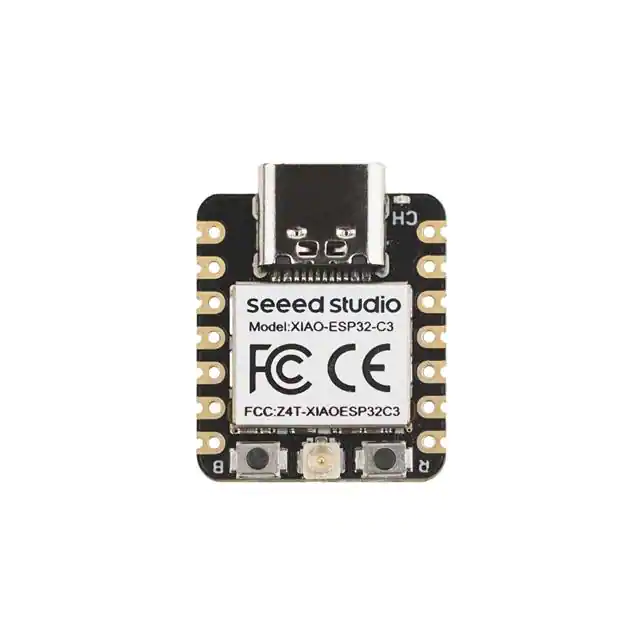
-
113991054
Seeed Technology Co., Ltd
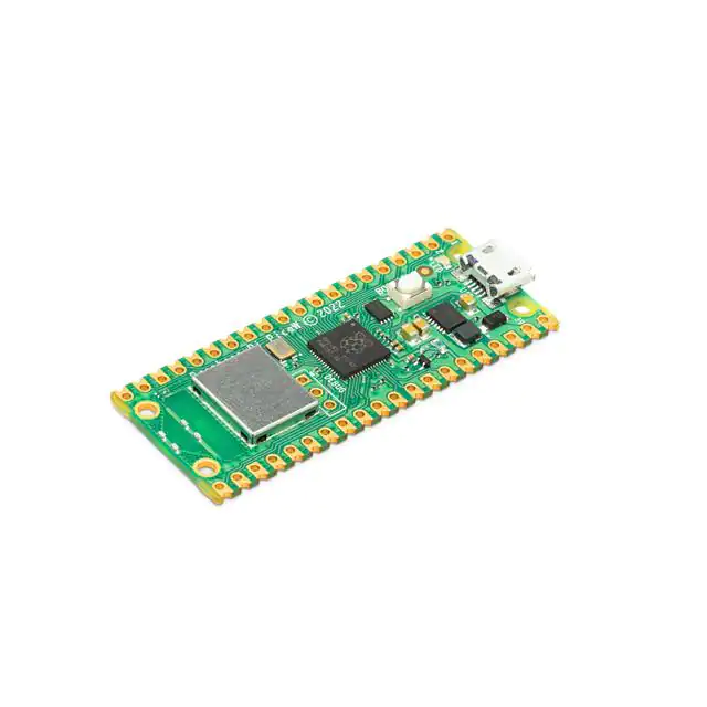
-
SC0918
Raspberry Pi

-
113991114
Seeed Technology Co., Ltd
-
ESP32-C6-DEVKITM-1-N4
Espressif Systems
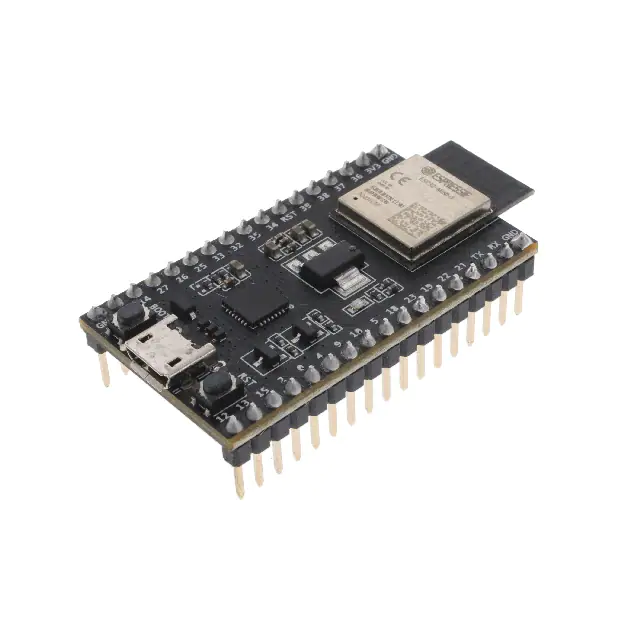
-
ESP32-DEVKITM-1
Espressif Systems
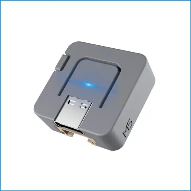
-
C008
M5Stack Technology Co., Ltd.
-
ESP32-C3-DEVKITC-02
Espressif Systems
-
ESP32-C6-DEVKITC-1-N8
Espressif Systems
-
DFR0478
DFRobot
-
102010448
Seeed Technology Co., Ltd
-
ESP32-DEVKITC-32E
Espressif Systems
-
ESP32-DEVKITC-32UE
Espressif Systems
Tech Hub

A practical engineering guide to 3.3V and 5V logic compatibility, input thresholds, resistor dividers, translator ICs, MOSFET level shifting, I2C pull-ups, timing limits and power-sequencing risks.

The 74HC595 uses push-pull logic outputs, while the TPIC6B595 uses 50 V open-drain DMOS sinks for higher-power loads. This guide compares timing, current limits, 3.3 V interfacing, load wiring, thermal…

The 74HC595 converts serial data into eight stable parallel outputs. This guide covers pin functions, shift and storage timing, OE and MR behavior, drive-current limits, cascading, voltage compatibilit…

A technical comparison of level-sensitive latches and edge-triggered flip-flops, covering timing windows, setup and hold limits, master–slave operation, time borrowing, race-through, HDL inference and…

A D latch stores one bit while Enable controls when data can pass. This reference covers gate-level operation, truth tables, transparency, setup and hold timing, LE versus OE, common ICs and practical …

An SR latch stores one bit through cross-coupled feedback. This engineering reference covers NOR and NAND implementations, truth tables, forbidden-state recovery, gated operation, switch debouncing, fa…

Latch circuits retain one bit through feedback. This technical reference covers SR and D latches, truth tables, transparency, timing limits, latch-versus-flip-flop behavior, applications and common log…

An engineering guide to LED driver operation, constant-current and constant-voltage outputs, linear and switching topologies, dimming, IC selection, calculations, replacement compatibility, and fault c…

Operational amplifier guide covering op amp basics, feedback, ideal vs real op amps, common configurations, buffer circuits, offset, bias current, gain-bandwidth, slew rate, rail-to-rail limits and sel…

Jumper cables guide covering safe connection order, red and black clamp placement, final ground connection, cable gauge, length, clamp quality, copper vs CCA cables, jump starter comparison and battery…


