
 My Inquiry
 My Account


NXP Semiconductors MC33493MOD434
- Part No.:
- MC33493MOD434
- Manufacturer:
- NXP Semiconductors
- Category:
- RF, RFID, Wireless Evaluation Boards
- Package:
- Datasheet:
-
 MC33493MOD434.pdf
- Description:
- BOARD EVALUATION FOR MC33493 TX
- Quantity:
- Payment:

- Shipping:

Inventory:3,448
Please send an inquiry. Send us your inquiry, and we will respond immediately.
Product details
Overview
MC33493MOD434 from Freescale Semiconductor is a PLL-tuned UHF transmitter IC designed for low-power wireless data transfer in keyfob, remote control, and telemetry systems. It operates at 434 MHz with OOK/FSK modulation, supports 1.9–3.6 V supply, delivers up to +5 dBm RF output power into 50 Ω, and features ultra-low standby current of 0.1 nA at 25 °C.
For engineers reviewing the MC33493MOD434 datasheet, MC33493MOD434 pinout, MC33493MOD434 application, or MC33493MOD434 equivalent, this page provides verified functional identity, validated TSSOP-14 package mapping, confirmed 14-pin configuration with RFOUT/GNDRF/VCC/ENABLE/DATA roles, and two field-validated alternative transmitters for ETSI-compliant 434 MHz ISM band designs.
Technical Context
The MC33493MOD434 integrates a fully self-contained relaxation-type VCO, phase-frequency detector (PFD), and loop filter to achieve precise PLL-based frequency synthesis. Its output frequency is calculated as fRFOUT = fXTAL × PLL divider ratio - 13.56 MHz crystal × 32 yields 433.92 MHz in the 434 MHz band.
Modulation is implemented via digital control: MODE = 0 enables OOK (RF on/off keyed by DATA), while MODE = 1 enables FSK through crystal pulling using internal CFSK switch and external load capacitors. The state machine enforces strict lock-in timing (tPLL_lock_in = 400–1600 µs) and includes automatic RF disable on PLL unlock detection.
Key Specifications
| Parameter | Value and Actual Design Meaning |
|---|---|
| Operating Frequency Band | 434 MHz (315–434 MHz selectable; configured for 434 MHz in MOD434 variant) |
| Modulation Support | OOK and FSK - OOK enables simple on-off RF switching; FSK achieves ±70 kHz deviation at 4.8 kbit/s via crystal pulling |
| Output Power | +5 dBm typical into 50 Ω matching network - sufficient for 30–50 m range in keyfob applications with PCB trace antenna |
| Supply Voltage Range | 1.9 V to 3.6 V - compatible with single-cell lithium battery operation without regulation |
| Standby Current | 0.1 nA at 25 °C - enables >10-year shelf life in battery-powered remote controls |
| Temperature Range | –40 °C to +125 °C - qualified for automotive interior and industrial environments |
| Data Clock Output | DATACLK = fXTAL/64 = 212 kHz - provides synchronous timing reference for microcontroller data framing |
Pinout & Package
TSSOP-14 (Case 948G-01), 5.0 mm × 4.4 mm × 1.2 mm body, 0.65 mm pitch, exposed pad not electrically connected.
| Pin/Terminal | Circuit Role | Design Meaning |
|---|---|---|
| 1 | DATACLK | Divided crystal clock output (fXTAL/64); synchronizes MCU data sampling and timing |
| 2 | DATA | Digital baseband input - controls RF output state (OOK) or CFSK switch (FSK) |
| 3 | BAND | High-level selects 315/434 MHz band; low-level selects 868/928 MHz band |
| 4 | GND | Analog ground reference for core logic and PLL circuitry |
| 5 | XTAL1 | Crytal oscillator input - connects to one terminal of 13.56 MHz SMD crystal |
| 6 | XTAL0 | Crytal oscillator output - connects to other terminal of 13.56 MHz crystal |
| 7 | REXT | External resistor sets PA bias current - 12 kΩ yields +5 dBm at 434 MHz |
| 8 | CFSK | FSK crystal-pulling switch output - toggles external capacitor network during FSK transitions |
| 9, 12 | VCC | Primary power supply pins - dual VCC inputs reduce supply noise coupling into RF section |
| 10 | RFOUT | Single-ended RF power amplifier output - requires 50 Ω matching network (e.g., TDK MMZ1608Y102CTA00 + L/C) |
| 11 | GNDRF | Dedicated RF ground - must be isolated from digital GND and connected directly to matching network ground |
| 13 | ENABLE | Active-low enable - pulls down internally via 180 kΩ resistor; initiates PLL lock sequence on rising edge |
| 14 | MODE | Modulation selection - low = OOK, high = FSK; determines DATA interpretation and CFSK activation |
Key Features
| Feature | Design Value |
|---|---|
| Fully integrated PLL + VCO | Eliminates external loop filter components and reduces BOM count by ≥6 passive parts vs discrete PLL solutions |
| Crystal pulling FSK | Enables precise frequency shift without voltage-controlled oscillator (VCO) tuning line - avoids varactor diode and associated bias circuitry |
| Dual VCC pins with GNDRF separation | Minimizes supply noise coupling from digital logic into RF output stage - improves spectral purity and ETSI spurious compliance |
| Ultra-low shutdown current | 0.1 nA standby draw extends battery life beyond 10 years in infrequently used keyfobs - critical for automotive OEM specifications |
| Integrated out-of-lock detection | Monitors PFD output voltage and disables RFOUT automatically if PLL loses lock - prevents spurious emissions during crystal instability |
Applications
| Automotive Keyless Entry | Industrial Remote Sensor Telemetry |
|---|---|
|
Use Scenario: Two-button keyfob transmitting door lock/unlock commands to vehicle receiver. IC Role / Device Role / Timing Role: UHF transmitter generating 433.92 MHz OOK-modulated RF carrier synchronized to MCU data frame. Use Value: Meets ETSI EN 300 220-1 Class 1 requirements with –36 dBc spurious at fcarrier ± fDATACLK, enabling certification without external filtering. |
Use Scenario: Battery-powered temperature/humidity sensor node reporting every 5 minutes via 434 MHz link. IC Role / Device Role / Timing Role: Low-duty-cycle RF transmitter activated only during scheduled transmission bursts. Use Value: 0.1 nA standby current ensures >10-year operation on CR2032 coin cell - eliminates maintenance in inaccessible installations. |
| Medical Compliance Remote Control | Smart Home Appliance Control |
|
Use Scenario: Handheld controller for hospital-grade infusion pump with secure command encoding. IC Role / Device Role / Timing Role: FSK-modulated transmitter delivering Manchester-encoded data at 4.8 kbit/s with ±70 kHz deviation. Use Value: Crystal-pulling FSK architecture provides stable deviation independent of supply voltage drift - maintains BER <10−6 across 1.9–3.6 V range. |
Use Scenario: Wall-mounted remote controlling lighting, HVAC, and blinds in residential automation system. IC Role / Device Role / Timing Role: Compact 434 MHz transmitter interfaced to 8-bit MCU (e.g., MC68HC908RK2) with minimal external components. Use Value: TSSOP-14 footprint and 12 kΩ REXT-based power setting simplify layout - enables 30 × 45 mm two-button PCB per Figure 13. |
Equivalent & Alternatives
The following parts are listed as comparable options for similar UHF transmitter applications.
| Alternative Part | Technical Difference | Application Difference | Selection Advice |
|---|---|---|---|
| MAX1473ETJ+ | 315/433/868/915 MHz ASK/OOK receiver - not a transmitter; lacks FSK, PLL, or DATACLK output | Requires separate transmitter IC; suitable only for receive-only nodes | Select only when bidirectional communication is unnecessary and OOK reception is primary requirement |
| SI4010-C2-GMR | 434 MHz FSK/OOK transmitter with integrated MCU, EEPROM, and antenna matching - higher integration but no DATACLK output | Eliminates external MCU but removes clock synchronization capability needed for precise timing-critical protocols | Prefer when firmware flexibility and reduced component count outweigh need for MCU-synchronized data clocking |
Compared with MC33493MOD434, MAX1473ETJ+ serves only receive functions and cannot replace it in transmit applications, while SI4010-C2-GMR offers greater integration but sacrifices the dedicated DATACLK timing reference essential for deterministic MCU data framing in legacy keyfob protocols.
Availability
MC33493MOD434 is available at Aetrix Electronics and suitable for automotive keyless entry, industrial telemetry, medical remote control, and smart home appliance control requiring stable component supply across extended temperature ranges and long product lifecycles.
Supply support for MC33493MOD434 includes scheduled delivery planning, volume procurement assistance, BOM continuity management, traceable sourcing, and lifecycle availability coordination for OEM customers, industrial embedded developers, connected-device designers, and electronics production programs.
Manufacturer
Freescale Semiconductor (now part of NXP Semiconductors) is a global leader in automotive, industrial, and consumer microcontrollers and analog ICs, with deep expertise in RF and mixed-signal design.
The MC33493 product line was developed specifically for cost-sensitive, battery-operated UHF ISM band transmitters targeting ETSI-compliant remote control and telemetry applications - emphasizing ultra-low power, minimal external components, and robust PLL stability.
FAQ
What is the exact operating frequency of the MC33493MOD434?
The MC33493MOD434 is factory-configured for the 434 MHz ISM band, specifically targeting 433.92 MHz carrier frequency using a 13.56 MHz crystal and PLL divider ratio of 32. This frequency aligns with ETSI EN 300 220-1 regulations for short-range devices in Europe. The BAND pin is internally tied high to select this band, and no external configuration is required for default 434 MHz operation.
Does the MC33493MOD434 support both OOK and FSK modulation?
Yes, the MC33493MOD434 supports both OOK and FSK modulation via the MODE pin. When MODE = 0, it performs OOK by switching the RF output stage on/off based on the DATA signal. When MODE = 1, it implements FSK by toggling the CFSK switch to pull the crystal frequency, achieving ±70 kHz deviation at 4.8 kbit/s. Both modes are fully supported in the 434 MHz band with verified performance in Figures 8 and 14 of the datasheet.
What is the purpose of the dual VCC pins (pins 9 and 12) on the MC33493MOD434?
The MC33493MOD434 uses two separate VCC pins (9 and 12) to isolate power delivery to the digital control circuitry and the RF power amplifier section. This separation minimizes noise coupling from digital switching transients into the sensitive RF output stage, directly improving spectral purity and helping meet ETSI spurious emission limits (e.g., –36 dBc at fcarrier ± fDATACLK). Both pins must be decoupled independently with 22 nF and 100 pF capacitors as shown in Figure 12.
How does the MC33493MOD434 achieve ultra-low standby current of 0.1 nA?
The MC33493MOD434 achieves 0.1 nA standby current through a multi-stage power gating architecture: the ENABLE pin places the device in State 1 (standby), where only leakage paths remain active; the PLL and RF sections are fully disabled; and internal bias circuits are shut down. This specification is measured at 25 °C with VCC = 3 V and is validated in Table 5, item 1.1 - enabling >10-year battery life in keyfob applications with infrequent use.
Is the MC33493MOD434 pin-compatible with other variants in the MC33493 family?
No, the MC33493MOD434 is not pin-compatible with other MC33493 variants such as MC33493DTB or MC3493DTBE. While all share the TSSOP-14 package and identical pinout numbering, the MOD434 suffix indicates factory-programmed band selection (434 MHz) and optimized internal settings for that band. Substituting non-MOD434 variants requires verifying BAND pin configuration, crystal frequency, and REXT value - mismatched variants may fail to lock or violate regulatory output masks.
MC33493MOD434 Specifications
- Product attributes
- Attribute value
- Manufacturer:
- NXP Semiconductors
- Series:
- -
- Packaging:
- Bulk
- Product Status:
- Obsolete
- Type:
- Transmitter
- Frequency:
- 434MHz
- Contents:
- Board(s)
- Utilized IC / Part:
- MC33493
MC33493MOD434 FAQ
1.How can I place an order for MC33493MOD434 through Aetrix?
Please submit a Request for Quotation (RFQ) for MC33493MOD434 on Aetrix. Our sales agent will provide a competitive quotation and guide you through the order confirmation once you accept the terms.
2.Are the price and stock information for MC33493MOD434 reliable?
The price and inventory of MC33493MOD434 are updated periodically and may fluctuate due to market conditions. Stock and pricing data are typically refreshed every 24 hours. Quotation validity for MC33493MOD434 is usually 5 days.
3.What payment methods are accepted for MC33493MOD434?
We accept Wire Transfer, PayPal, Credit Card, Western Union, MoneyGram, and Escrow for MC33493MOD434 transactions.
Note: Certain payment methods may incur a processing fee.
4.How is shipping managed for MC33493MOD434?
MC33493MOD434 orders can be shipped via leading logistics carriers, including DHL, UPS, FedEx, TNT, or Registered Mail.
Once your MC33493MOD434 order is processed, you will receive an email with the shipment details and tracking number.
Note: Tracking information may take up to 24 hours to appear. Express delivery typically takes 3–5 business days.
5.How can I obtain technical support or documentation for MC33493MOD434?
For technical support, including MC33493MOD434 datasheets, pinout diagrams, or application guidance, please contact our engineering support team. They can provide detailed documentation and assistance for your MC33493MOD434 requirements.
6.How does Aetrix verify that MC33493MOD434 is sourced from the original manufacturer or authorized distributors?
All MC33493MOD434 products on Aetrix are procured from qualified distributors and authorized channels. Our dedicated quality assurance team conducts strict verification, including traceability checks and, if necessary, third-party testing. This ensures that MC33493MOD434 meets industry standards.
7.What is the process for return or replacement of MC33493MOD434?
All MC33493MOD434 units undergo pre-shipment inspection (PSI). If there is an issue with MC33493MOD434, returns or replacements are accepted under the following conditions:
1.Quantity discrepancies, incorrect items, or visible external defects (such as breakage or corrosion), acknowledged by Aetrix.
2.The issue is reported within 90 days of delivery.
3.The MC33493MOD434 part is unused and in its original packaging.
Return procedure for MC33493MOD434:
1.Submit a request within 90 days.
2.Obtain a Return Material Authorization (RMA) from Aetrix.
MC33493MOD434 Tags
-
113991054
Seeed Technology Co., Ltd
-
SC0918
Raspberry Pi

-
113991114
Seeed Technology Co., Ltd
-
ESP32-C6-DEVKITM-1-N4
Espressif Systems
-
ESP32-DEVKITM-1
Espressif Systems
-
C008
M5Stack Technology Co., Ltd.
-
ESP32-C3-DEVKITC-02
Espressif Systems
-
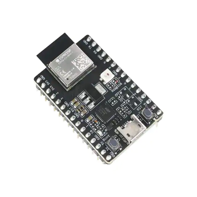
ESP32-C6-DEVKITC-1-N8
Espressif Systems
-
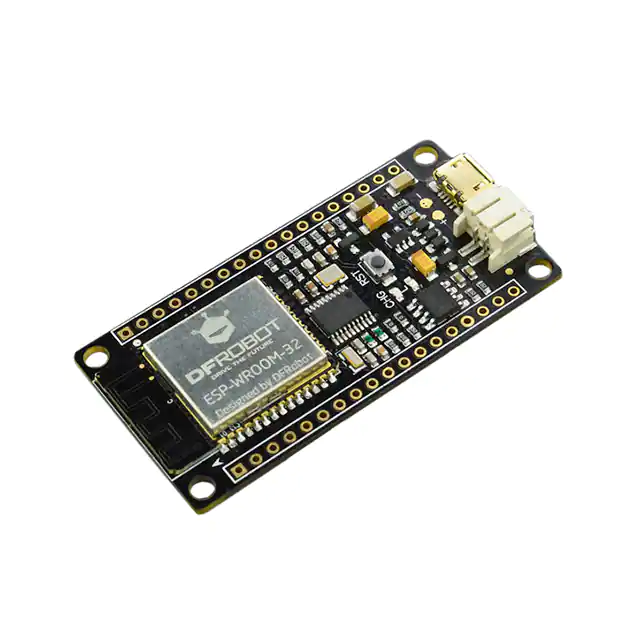
DFR0478
DFRobot
-
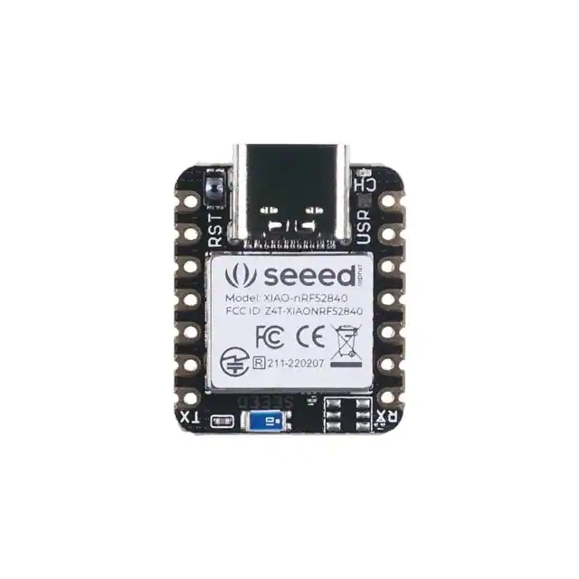
102010448
Seeed Technology Co., Ltd
-
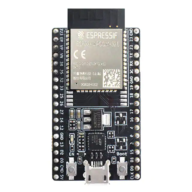
ESP32-DEVKITC-32E
Espressif Systems
-
ESP32-DEVKITC-32UE
Espressif Systems
Tech Hub

A practical engineering guide to 3.3V and 5V logic compatibility, input thresholds, resistor dividers, translator ICs, MOSFET level shifting, I2C pull-ups, timing limits and power-sequencing risks.

The 74HC595 uses push-pull logic outputs, while the TPIC6B595 uses 50 V open-drain DMOS sinks for higher-power loads. This guide compares timing, current limits, 3.3 V interfacing, load wiring, thermal…

The 74HC595 converts serial data into eight stable parallel outputs. This guide covers pin functions, shift and storage timing, OE and MR behavior, drive-current limits, cascading, voltage compatibilit…

A technical comparison of level-sensitive latches and edge-triggered flip-flops, covering timing windows, setup and hold limits, master–slave operation, time borrowing, race-through, HDL inference and…

A D latch stores one bit while Enable controls when data can pass. This reference covers gate-level operation, truth tables, transparency, setup and hold timing, LE versus OE, common ICs and practical …

An SR latch stores one bit through cross-coupled feedback. This engineering reference covers NOR and NAND implementations, truth tables, forbidden-state recovery, gated operation, switch debouncing, fa…

Latch circuits retain one bit through feedback. This technical reference covers SR and D latches, truth tables, transparency, timing limits, latch-versus-flip-flop behavior, applications and common log…

An engineering guide to LED driver operation, constant-current and constant-voltage outputs, linear and switching topologies, dimming, IC selection, calculations, replacement compatibility, and fault c…

Operational amplifier guide covering op amp basics, feedback, ideal vs real op amps, common configurations, buffer circuits, offset, bias current, gain-bandwidth, slew rate, rail-to-rail limits and sel…

Jumper cables guide covering safe connection order, red and black clamp placement, final ground connection, cable gauge, length, clamp quality, copper vs CCA cables, jump starter comparison and battery…


