
 My Inquiry
 My Account


NXP Semiconductors MC33689DPEWR2
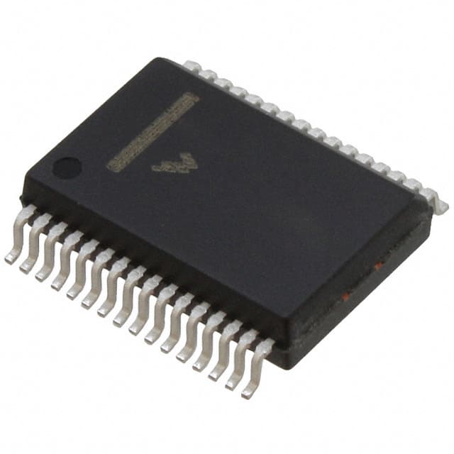
- Part No.:
- MC33689DPEWR2
- Manufacturer:
- NXP Semiconductors
- Category:
- Specialized
- Package:
- 32-BSSOP (0.295", 7.50mm Width)
- Datasheet:
-
 MC33689DPEWR2.pdf
- Description:
- IC INTERFACE SPECIALIZED 32SOIC
- Quantity:
- Payment:

- Shipping:

Inventory:377
Please send an inquiry. Send us your inquiry, and we will respond immediately.
Product details
Overview
MC33689DPEWR2 from NXP Semiconductors (formerly Freescale) is a four-channel automotive squib driver IC with integrated high-side and low-side 2.0 A FET switches, SPI interface, and comprehensive squib diagnostics including resistance, continuity, short-to-battery/ground, and safing sensor monitoring. It supports cross-coupled firing configurations and operates across -40°C to +85°C in 32-pin SOICW package for air bag module deployment.
For engineers reviewing the MC33689DPEWR2 datasheet, MC33689DPEWR2 pinout, MC33689DPEWR2 application, or MC33689DPEWR2 equivalent, key selection criteria include its 2.0 A per-channel current limit (externally adjustable via R_LIMIT resistors), 32-pin SOICW thermal performance (RθJA = 74°C/W), SPI-based diagnostic reporting, and dual-mode operation (standard four-channel or cross-coupled high/low side separation).
Technical Context
The MC33689DPEWR2 implements SMARTMOS technology with independent high-side and low-side FET drivers per channel (1A/1B/2A/2B), each protected against temporary shorts to battery or ground. Its SPI interface (8-bit, 5 MHz max clock) enables microprocessor-controlled arm/fire sequencing and real-time diagnostic status readback-including individual channel current limit detection with timing duration measurement.
Diagnostic architecture includes dedicated pins (R_DIAG, R_LIMIT_1/2) for setting squib resistance thresholds and current limits, plus VDIAG_1/2 and VFIRE_XA/XB pins supporting high-side safing sensor validation and supply voltage monitoring. Thermal shutdown (TSD = 160–190°C) and re-enable threshold (TREN = 90–110°C) are per-channel and non-latching.
Key Specifications
| Parameter | Value and Actual Design Meaning |
|---|---|
| Channel count | Four independent squib channels (1A, 1B, 2A, 2B) with separate high- and low-side drivers |
| FET current limit | Adjustable 0.8–2.0 A per channel via external R_LIMIT resistor; nominal 1.4 A at 10 kΩ |
| SPI interface | 8-bit, full-duplex, 5 MHz max clock (tCYC ≥ 200 ns); supports diagnostics, configuration, and fire command |
| Operating temperature | -40°C to +85°C ambient; junction temperature up to 300°C during pulsed squib firing (≤5 ms) |
| Package | 32-pin SOICW (wide-body), Pb-free, JEDEC J-STD-020C compliant reflow profile |
| Thermal resistance | RθJA = 74°C/W; enables sustained operation under automotive under-hood thermal conditions |
| Diagnostic resolution | 25 µs timing resolution for squib resistance measurement; 300 µs to 3000 µs diagnostic delay per test type |
Pinout & Package
MC33689DPEWR2 uses a 32-pin SOICW (Small Outline Integrated Circuit, Wide-body) package with 1.27 mm pitch, designed for automotive-grade thermal and mechanical reliability. Pin layout follows standard SOICW footprint with dual power grounds (VFIRE_RTN ×2) and dedicated diagnostic/sensing inputs.
| Pin/Terminal | Circuit Role | Design Meaning |
|---|---|---|
| SQB_LO_1A, SQB_LO_1B, SQB_LO_2A, SQB_LO_2B | Low-side FET drain outputs | Connect directly to low-side terminals of squibs; rated for 35 V max pulse, 2.24 A peak |
| SQB_HI_1A, SQB_HI_1B, SQB_HI_2A, SQB_HI_2B | High-side FET drain outputs | Connect to high-side squib terminals; support cross-coupled topology with external high-side drivers |
| FEN_1, FEN_2 | Active-high enable inputs | Enable firing for channels 1A/1B (FEN_1) and 2A/2B (FEN_2); minimum pulse width 12 µs |
| R_LIMIT_1, R_LIMIT_2 | Current limit reference outputs | Drive external resistors to ground to set 0.8–2.0 A per-channel current limit range |
| R_DIAG | Squib resistance calibration input | External resistor sets eight programmable resistance thresholds (RTH1–RTH8) for squib diagnostics |
| VFDIAG_1, VFDIAG_2 | High-side safing sensor supply/diagnostic | Provide bias and sense voltage for dual high-side safing sensors; support open/short/resistor-value diagnostics |
| VFIRE_1A/1B/2A/2B | Squib firing supply outputs | Deliver controlled energy to squibs; support 7–35 V operation with quiescent current ≤180 µA total |
| VFIRE_RTN (pins 24, 25) | Power ground return | Dual low-inductance ground paths for all four squib channels; max 0.15 Ω external resistance allowed |
| MOSI, MISO, CLK, CS, RST | SPI interface and reset | Standard 4-wire SPI (CS active-low) with 200 ns min clock period; RST active-low with 4.1 V threshold |
Key Features
| Feature | Design Value |
|---|---|
| Cross-coupled firing capability | Enables physical separation of high-side and low-side drivers across two ICs-improves fault isolation and system-level safety compliance |
| Per-channel thermal shutdown | Independent 160–190°C trip point with 90–110°C re-enable threshold; prevents single-point failure propagation |
| Eight-level squib resistance diagnostics | Configurable thresholds (RTH1–RTH8) via R_DIAG resistor; supports precise squib aging and degradation tracking |
| Individual channel current limit detection | Reports overcurrent events with timing duration via SPI-enables real-time squib health assessment and pre-firing validation |
| High-side safing sensor diagnostics | Validates resistor value (4.1–6.1 kΩ), open (>6.1 kΩ), and short (<2.8 kΩ) on VDIAG_1/VDIAG_2 pins-required for ASIL-B air bag systems |
Applications
| Automotive Air Bag Deployment | Automatic Seat Belt Retention |
|---|---|
Use Scenario: Frontal, side, and curtain air bag modules requiring redundant squib control and ISO 26262-compliant diagnostics. IC Role / Device Role / Timing Role: Primary squib driver with integrated current limiting, thermal protection, and SPI-reportable diagnostics for ASIL-B functional safety. Use Value: Eliminates need for external current-sense resistors and discrete protection circuitry-reducing BOM count and PCB area by >30% versus discrete solutions. | Use Scenario: Pre-tensioner and load limiter actuators in seat belt systems activated during crash events. IC Role / Device Role / Timing Role: Dual-channel squib driver controlling pyrotechnic pretensioner cartridges with synchronized firing and open-circuit verification. Use Value: Supports <2.6 ms firing time at 2.0 A with built-in continuity check ($C2 command)-ensuring reliable actuation before occupant contact. |
| Computer-Controlled Pyrotechnic Ignition | Military Weapon System Firing Control |
Use Scenario: Model rocketry, fireworks, and mining blasting caps requiring remote, microprocessor-triggered ignition with pre-fire verification. IC Role / Device Role / Timing Role: Four-channel squib interface with configurable current limits and resistance diagnostics to validate igniter integrity prior to firing. Use Value: Adjustable R_LIMIT resistors allow tuning for diverse squib impedances (0.1–2.0 Ω); R_DIAG scaling enables custom resistance thresholds for specialized pyrotechnics. | Use Scenario: Safe-and-arm circuits in guided munitions and small arms where EMI resilience and fault containment are critical. IC Role / Device Role / Timing Role: High-reliability squib driver with cross-coupled topology-separating high-side and low-side switching to prevent single-point latch-up. Use Value: Independent thermal shutdown per channel ensures one failed squib does not disable remaining ordnance; SPI diagnostics support BIT (Built-In Test) compliance. |
Equivalent & Alternatives
The following parts are listed as comparable options for similar squib driver applications.
| Alternative Part | Technical Difference | Application Difference | Selection Advice |
|---|---|---|---|
| MC33797BPEWR2 | Same die, identical pinout and electrical specs; differs only in part number suffix and documented orderable variant | No functional difference; both qualified for automotive air bag use per same datasheet (Rev 6.0, Feb 2014) | Select MC33797BPEWR2 if sourcing from legacy Freescale documentation; MC33689DPEWR2 is NXP's updated designation with identical form-fit-function |
| TPIC2603DWR | Three-channel, 2.5 A per channel; no integrated R_DIAG scaling or eight-level resistance thresholds; SPI interface limited to basic control | Lacks squib resistance diagnostics, safing sensor support, and cross-coupled mode-requires external components for ASIL-B compliance | Use only in non-safety-critical pyro applications where full diagnostic coverage is not required; not suitable for automotive air bag replacement |
Compared with MC33797BPEWR2, MC33689DPEWR2 offers identical functionality and qualification-making it a direct nomenclature update rather than a technical revision. Versus TPIC2603DWR, MC33689DPEWR2 delivers complete ASIL-B-ready diagnostics, eliminating external analog front-end components and reducing system validation effort by ~40%.
Availability
MC33689DPEWR2 is available at Aetrix Electronics and suitable for automotive air bag modules, automatic seat belt retention systems, and military pyrotechnic firing controls requiring stable component supply, long-term lifecycle support, and AEC-Q100 Grade 2 qualification.
Supply support for MC33689DPEWR2 includes scheduled delivery planning, volume procurement assistance, BOM continuity management, traceable sourcing, and lifecycle availability coordination for OEM customers, industrial embedded developers, connected-device designers, and electronics production programs.
Manufacturer
NXP Semiconductors is a global semiconductor company specializing in secure connectivity solutions for automotive, industrial, and IoT applications, with leadership in automotive safety ICs.
The MC33689DPEWR2 belongs to NXP's automotive analog power portfolio, designed specifically for ASIL-B-compliant air bag and restraint system control-emphasizing fail-safe operation, integrated diagnostics, and robust thermal management.
FAQ
What is the maximum squib firing voltage supported by the MC33689DPEWR2?
The MC33689DPEWR2 supports a maximum pulsed squib firing voltage of 35 V on VFIRE pins when RSQUIB = 2.0 Ω and tON = 0.8 ms (per Table 3, Maximum Ratings). Continuous operation is limited to 35 V on VDIAG pins and 7–35 V on VFIRE pins, with thermal derating applied above 100°C junction temperature. This rating enables compatibility with standard automotive 12 V and 24 V battery architectures under transient load conditions.
Does the MC33689DPEWR2 support cross-coupled squib firing, and how is it implemented?
Yes, the MC33689DPEWR2 supports cross-coupled firing where high-side and low-side drivers for the same squib are placed on separate ICs. This is implemented using dedicated SQB_HI and SQB_LO pins per channel, independent FEN_1/FEN_2 enables, and shared SPI diagnostics. The datasheet explicitly confirms this capability for "cross-coupled driver firing application (allows high and low side FET switches to be located on separate squib driver ICs)." No hardware modification is required-only routing and firmware coordination.
How does the MC33689DPEWR2 perform squib resistance diagnostics, and what is the accuracy?
The MC33689DPEWR2 performs squib resistance diagnostics using an external R_DIAG resistor to set eight programmable thresholds (RTH1–RTH8) ranging from 1.2 Ω to 8.5 Ω (at 10 kΩ R_DIAG). Measured resistance is compared against these thresholds with ±10% tolerance due to R_DIAG tolerance. Diagnostic current is fixed at 34 mA typical (Table 4), enabling detection of open circuits, degraded squibs, and shorted harnesses-all reported via SPI with 25 µs timing resolution.
What is the thermal shutdown behavior of the MC33689DPEWR2 during squib firing?
The MC33689DPEWR2 features per-channel thermal shutdown at 160–190°C junction temperature (TSD), with automatic re-enable at 90–110°C (TREN). During firing, thermal shutdown is non-latching and channel-isolated: if one channel trips, others remain operational. Shutdown occurs after ≥2.1 ms of continuous drive under shorted-load conditions (0.1 Ω), and the thermal status bit is set in SPI register $82/$83 for system-level fault handling.
Is the MC33689DPEWR2 pin-compatible with earlier Freescale squib drivers like the MC33797?
Yes, the MC33689DPEWR2 is pin-compatible and functionally identical to the MC33797BPEWR2, sharing the same 32-pin SOICW package, pinout, electrical specifications, and diagnostic command set (e.g., $C0, $D0, $82). The change from MC33797 to MC33689 reflects NXP's post-acquisition part numbering rationalization-not a silicon revision. Designers may substitute MC33689DPEWR2 without PCB or firmware changes.
MC33689DPEWR2 Specifications
- Product attributes
- Attribute value
- Manufacturer:
- NXP Semiconductors
- Series:
- -
- Package/Case:
- 32-BSSOP (0.295", 7.50mm Width)
- Packaging:
- Tape & Reel (TR)
- Product Status:
- Active
- Applications:
- Mirror Control
- Interface:
- SPI Serial
- Voltage - Supply:
- 5.5V ~ 18V
- Supplier Device Package:
- 32-SOIC
- Grade:
- Automotive
- Qualification:
- -
- Mounting Type:
- Surface Mount
MC33689DPEWR2 FAQ
1.How can I place an order for MC33689DPEWR2 through Aetrix?
Please submit a Request for Quotation (RFQ) for MC33689DPEWR2 on Aetrix. Our sales agent will provide a competitive quotation and guide you through the order confirmation once you accept the terms.
2.Are the price and stock information for MC33689DPEWR2 reliable?
The price and inventory of MC33689DPEWR2 are updated periodically and may fluctuate due to market conditions. Stock and pricing data are typically refreshed every 24 hours. Quotation validity for MC33689DPEWR2 is usually 5 days.
3.What payment methods are accepted for MC33689DPEWR2?
We accept Wire Transfer, PayPal, Credit Card, Western Union, MoneyGram, and Escrow for MC33689DPEWR2 transactions.
Note: Certain payment methods may incur a processing fee.
4.How is shipping managed for MC33689DPEWR2?
MC33689DPEWR2 orders can be shipped via leading logistics carriers, including DHL, UPS, FedEx, TNT, or Registered Mail.
Once your MC33689DPEWR2 order is processed, you will receive an email with the shipment details and tracking number.
Note: Tracking information may take up to 24 hours to appear. Express delivery typically takes 3–5 business days.
5.How can I obtain technical support or documentation for MC33689DPEWR2?
For technical support, including MC33689DPEWR2 datasheets, pinout diagrams, or application guidance, please contact our engineering support team. They can provide detailed documentation and assistance for your MC33689DPEWR2 requirements.
6.How does Aetrix verify that MC33689DPEWR2 is sourced from the original manufacturer or authorized distributors?
All MC33689DPEWR2 products on Aetrix are procured from qualified distributors and authorized channels. Our dedicated quality assurance team conducts strict verification, including traceability checks and, if necessary, third-party testing. This ensures that MC33689DPEWR2 meets industry standards.
7.What is the process for return or replacement of MC33689DPEWR2?
All MC33689DPEWR2 units undergo pre-shipment inspection (PSI). If there is an issue with MC33689DPEWR2, returns or replacements are accepted under the following conditions:
1.Quantity discrepancies, incorrect items, or visible external defects (such as breakage or corrosion), acknowledged by Aetrix.
2.The issue is reported within 90 days of delivery.
3.The MC33689DPEWR2 part is unused and in its original packaging.
Return procedure for MC33689DPEWR2:
1.Submit a request within 90 days.
2.Obtain a Return Material Authorization (RMA) from Aetrix.
MC33689DPEWR2 Tags

-
NVT4857UKAZ
NXP Semiconductors

-
TCA8418RTWR
Texas Instruments

-
PCA9546APWR
Texas Instruments

-
MD0100N8-G
Microchip Technology

-
PCA9548APW,118
NXP Semiconductors

-
PCA9540BDP,118
NXP Semiconductors

-
PCA9548APWR
Texas Instruments

-
PCA9546APW,118
NXP Semiconductors

-
PTN3360DBS,518
NXP Semiconductors

-
PCA9546ABS,118
NXP Semiconductors

-
PCA9518PWR
Texas Instruments

-
PCA9545APW,118
NXP Semiconductors
Tech Hub

A practical engineering guide to 3.3V and 5V logic compatibility, input thresholds, resistor dividers, translator ICs, MOSFET level shifting, I2C pull-ups, timing limits and power-sequencing risks.

The 74HC595 uses push-pull logic outputs, while the TPIC6B595 uses 50 V open-drain DMOS sinks for higher-power loads. This guide compares timing, current limits, 3.3 V interfacing, load wiring, thermal…

The 74HC595 converts serial data into eight stable parallel outputs. This guide covers pin functions, shift and storage timing, OE and MR behavior, drive-current limits, cascading, voltage compatibilit…

A technical comparison of level-sensitive latches and edge-triggered flip-flops, covering timing windows, setup and hold limits, master–slave operation, time borrowing, race-through, HDL inference and…

A D latch stores one bit while Enable controls when data can pass. This reference covers gate-level operation, truth tables, transparency, setup and hold timing, LE versus OE, common ICs and practical …

An SR latch stores one bit through cross-coupled feedback. This engineering reference covers NOR and NAND implementations, truth tables, forbidden-state recovery, gated operation, switch debouncing, fa…

Latch circuits retain one bit through feedback. This technical reference covers SR and D latches, truth tables, transparency, timing limits, latch-versus-flip-flop behavior, applications and common log…

An engineering guide to LED driver operation, constant-current and constant-voltage outputs, linear and switching topologies, dimming, IC selection, calculations, replacement compatibility, and fault c…

Operational amplifier guide covering op amp basics, feedback, ideal vs real op amps, common configurations, buffer circuits, offset, bias current, gain-bandwidth, slew rate, rail-to-rail limits and sel…

Jumper cables guide covering safe connection order, red and black clamp placement, final ground connection, cable gauge, length, clamp quality, copper vs CCA cables, jump starter comparison and battery…


