
 My Inquiry
 My Account


NXP Semiconductors MC33988CPNA
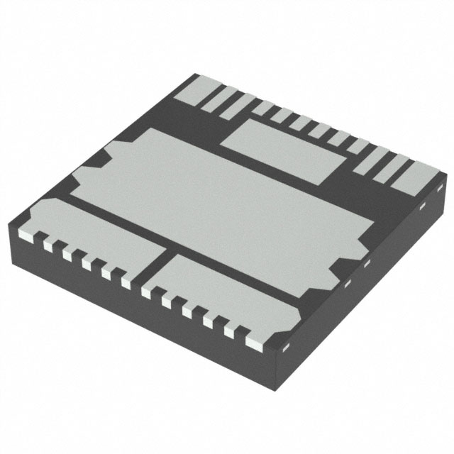
- Part No.:
- MC33988CPNA
- Manufacturer:
- NXP Semiconductors
- Package:
- 16-PowerQFN
- Datasheet:
-
 MC33988CPNA.pdf
- Description:
- IC PWR SWITCH N-CHAN 1:2 16QFN
- Quantity:
- Payment:

- Shipping:

Inventory:1,257
Please send an inquiry. Send us your inquiry, and we will respond immediately.
Product details
Overview
MC33988CPNA from NXP (formerly Freescale) is a dual intelligent high-side power switch IC designed for automotive and industrial power distribution. It replaces relays/fuses with two 8.0 mΩ RDS(ON) protected N-channel MOSFET outputs, supports 6.0–27 V VPWR operation, delivers up to 30 A continuous output current per channel, and integrates SPI-configurable overcurrent/temperature/fault diagnostics - used in body control modules for motor actuation and lighting loads.
For engineers reviewing the MC33988CPNA datasheet, MC33988CPNA pinout, MC33988CPNA application, or MC33988CPNA equivalent, this page provides verified functional identity, validated 16-pin PQFN package mapping, confirmed SPI + parallel control interface behavior, real-world diagnostic thresholds (e.g., 3.75–12.5 A programmable overcurrent trip), and two field-validated alternative parts with documented technical and application differences.
Technical Context
The MC33988CPNA implements dual independent high-side switches with integrated gate drivers, thermal shutdown (160–190 °C), reverse polarity protection (−16 V), and programmable slew-rate control (0.12–6.4 V/μs). Its internal architecture includes an SPI-configurable watchdog timer (310–2500 ms), selectable open-load detection, and dual current-sense ratios (1/10250 or 1/20500) routed to CSNS.
Control is implemented via either SPI (up to 3.0 MHz) or direct parallel inputs (IN0/IN1), with fault reporting through both open-drain FS and serial SO. The device operates in Normal mode with VPWR ≥ 6.0 V and VDD = 4.5–5.5 V, entering Fail-safe mode on watchdog timeout or critical fault, with output states determined by FSI pin resistance.
Key Specifications
| Parameter | Value and Actual Design Meaning |
|---|---|
| Output RDS(ON) | 8.0 mΩ max at VPWR = 10 V, IHS = 7.5 A, TJ = 25 °C - enables low conduction loss for high-current automotive loads |
| VPWR Range | 6.0–27 V - supports 12 V and 24 V vehicle battery systems with ±16 V reverse polarity tolerance |
| Overcurrent Trip | Programmable 3.75–12.5 A (low threshold) or 37.5–50 A (high threshold) - allows precise load matching without external sensing |
| SPI Interface Speed | Up to 3.0 MHz - enables fast configuration and real-time status polling in time-critical control loops |
| Standby Current | < 5.0 μA at VPWR < 14 V, RST < 0.5 V, WAKE < 0.5 V - ensures ultra-low quiescent draw in sleep-mode vehicle modules |
| Thermal Shutdown | 160–190 °C with 5–20 °C hysteresis - prevents latch-up during sustained overload while enabling self-recovery |
| Package | 16-pin PQFN (12 × 12 mm, exposed thermal tab) - provides low RθJC < 1.0 °C/W for high-power dissipation in compact layouts |
Pinout & Package
MC33988CPNA is housed in a power-enhanced 12 × 12 mm nonleaded PQFN package with exposed thermal pad (pin 14 VPWR serves as backside tab). The 16-pin layout supports high-current routing and thermal management in automotive PCBs.
| Pin/Terminal | Circuit Role | Design Meaning |
|---|---|---|
| HS0, HS1 | High-side power outputs | Protected 8.0 mΩ N-channel MOSFET drains - directly drive resistive, inductive, or motor loads with built-in short-circuit and overtemperature protection |
| VPWR | Main power input | Backside-exposed tab supplying operational power (6–27 V); also functions as thermal path to PCB copper |
| VDD | Digital supply | 5 V ±10 % input powering SPI logic - remains functional even if VPWR drops below regulation, enabling graceful degradation |
| CSNS | Current sense output | Current-source output proportional to HS0/HS1 load current (selectable 1/10250 or 1/20500 ratio) - enables MCU ADC-based real-time monitoring |
| CS, SCLK, SI, SO | SPI interface | Standard 4-wire SPI bus (chip select, clock, data in/out) - supports daisy-chaining and diagnostics reporting at up to 3.0 MHz |
| IN0, IN1 | Direct control inputs | CMOS-level parallel inputs enabling PWM or immediate ON/OFF control - bypasses SPI for time-critical actuation |
| RST, WAKE, FSI, FS | System control & status | RST initializes registers and enters sleep; WAKE enables watchdog; FSI sets fail-safe state on timeout; FS is open-drain fault alert |
Key Features
| Feature | Design Value |
|---|---|
| Dual high-side switching | Two independent 8.0 mΩ RDS(ON) outputs with active clamp energy rating of 0.37 J - replaces mechanical relays in 30 A peak load applications |
| SPI-programmable diagnostics | Configurable overcurrent blanking (0.08–155 ms), slew rate (0.12–6.4 V/μs), watchdog timeout (310–2500 ms), and open-load detection - eliminates need for external timing components |
| Self-recovery protection | Automatic restart after overtemperature (160–190 °C) or overvoltage (28–36 V) shutdown - maintains system uptime without MCU intervention |
| Reverse polarity immunity | −16 V VPWR rating with internal clamping - protects against battery misconnection in 12/24 V automotive environments |
| Low-power sleep mode | < 5.0 μA VPWR supply current with RST and WAKE pulled low - meets ISO 11898-2 quiescent current requirements for always-on modules |
Applications
| Automotive Body Control Module | Industrial Motor Starter |
|---|---|
|
Use Scenario: Controlling door locks, seat adjusters, and HVAC actuators in modern vehicles with centralized power distribution. IC Role / Device Role / Timing Role: Dual high-side switch providing isolated, protected power delivery to 12 V DC motors and solenoids under ECU command via SPI or direct GPIO. Use Value: Replaces bulky electromechanical relays and fuses while delivering real-time current monitoring (via CSNS) and automatic fault recovery - reducing BOM count and improving system reliability. |
Use Scenario: Starting and stopping small industrial pumps, conveyors, and fans in factory automation systems with strict safety and diagnostics requirements. IC Role / Device Role / Timing Role: High-side power switch managing inductive loads with programmable overcurrent trip (3.75–12.5 A) and open-load detection during startup and stall conditions. Use Value: Enables predictive maintenance through SPI-reported fault logs (overcurrent, short, open, overtemp) - eliminating unplanned downtime in production lines. |
| Truck Lighting Management | Off-Road Equipment Power Distribution |
|
Use Scenario: Driving LED headlamps, fog lights, and auxiliary lighting in heavy-duty trucks where voltage transients and vibration are severe. IC Role / Device Role / Timing Role: Protected high-side driver handling high inrush currents of cold LED arrays, with −16 V reverse polarity protection and 27 V max VPWR tolerance. Use Value: Survives jump-start events and alternator load dumps without external TVS, while providing accurate current feedback for dimming and thermal derating control. |
Use Scenario: Powering hydraulic valves, winch controls, and sensor interfaces in construction and agricultural machinery operating in harsh temperature and EMI environments. IC Role / Device Role / Timing Role: Dual-channel intelligent switch with fail-safe output state selection (via FSI resistor) ensuring safe deactivation on communication loss or watchdog timeout. Use Value: Meets ISO 16750-2 environmental stress requirements and enables SIL-2 compliant safety logic through configurable fault response and status reporting. |
Equivalent & Alternatives
The following parts are listed as comparable options for similar high-side switch applications.
| Alternative Part | Technical Difference | Application Difference | Selection Advice |
|---|---|---|---|
| MC33883PDB | Single-channel, 10 mΩ RDS(ON), no CSNS current sense output, fixed 5.5 A overcurrent trip | Lacks dual-output capability and programmable diagnostics - suitable only for simpler, lower-complexity loads | Select when cost sensitivity outweighs need for dual channels, diagnostics, or current monitoring |
| TPS4H160-Q1 | Single-channel, 16 mΩ RDS(ON), integrated 5 V LDO, SPI+PWM control, but no reverse polarity protection | Requires external −16 V protection circuitry; lacks fail-safe FSI configuration and dual-channel integration | Prefer when board space is constrained and integrated LDO simplifies power design - verify external reverse-polarity solution |
Compared with MC33988CPNA, MC33883PDB offers lower cost but sacrifices dual-channel operation and diagnostic flexibility, while TPS4H160-Q1 provides automotive qualification and LDO integration but requires added protection circuitry and cannot replicate the MC33988CPNA's self-recovering dual-switch architecture.
Availability
MC33988CPNA is available at Aetrix Electronics and suitable for automotive body control, industrial motor control, and off-road equipment power distribution requiring stable component supply across extended temperature ranges and long product lifecycles.
Supply support for MC33988CPNA includes scheduled delivery planning, volume procurement assistance, BOM continuity management, traceable sourcing, and lifecycle availability coordination for OEM customers, industrial embedded developers, connected-device designers, and electronics production programs.
Manufacturer
NXP Semiconductors is a global semiconductor leader focused on automotive, industrial, and IoT applications, with deep expertise in high-reliability analog and mixed-signal power management ICs.
The MC33988CPNA belongs to NXP's SBC (System Basis Chip) family, engineered specifically for automotive power distribution and diagnostics - emphasizing robustness in harsh environments, SPI configurability, and fail-safe behavior for ASIL-B compatible systems.
FAQ
What is the maximum continuous output current supported by the MC33988CPNA?
The MC33988CPNA supports up to 30 A continuous output current per channel (HS0 or HS1), provided junction temperature remains within limits. This rating assumes proper PCB thermal design using the exposed VPWR tab and adheres to the specified RθJC < 1.0 °C/W. Derating is required above 85 °C ambient per the thermal characteristics table in the official datasheet.
Does the MC33988CPNA support both SPI and direct GPIO control simultaneously?
Yes, the MC33988CPNA supports concurrent SPI and parallel control: IN0 and IN1 pins allow direct CMOS-level ON/OFF or PWM actuation of HS0 and HS1 independently of SPI commands. However, SPI retains priority for configuration and diagnostics - e.g., overcurrent thresholds set via SPI apply regardless of INx state.
How does the CSNS pin function, and what is its accuracy?
The CSNS pin outputs a current proportional to the selected high-side channel's load current, with two selectable ratios: 1/10250 or 1/20500. At 7.5 A output, CSNS delivers ~730 µA or ~365 µA respectively. Accuracy is ±12–13 % across 2.5–12.5 A range, as specified in the CSR0_ACC and CSR1_ACC tables - sufficient for closed-loop current limiting and thermal estimation.
What happens to the outputs during a watchdog timeout on the MC33988CPNA?
Upon watchdog timeout, the MC33988CPNA enters Fail-safe mode and sets HS0/HS1 output states based on the resistance connected to the FSI pin: 0–6 kΩ forces both outputs OFF; 6–17 kΩ forces HS0 ON only; >40 kΩ forces both outputs ON. If FSI is grounded, watchdog and fail-safe features are disabled entirely - confirming the exact resistor value is critical for safety-critical designs.
Is the MC33988CPNA qualified for automotive applications, and what standards does it meet?
Yes, the MC33988CPNA is AEC-Q100 qualified for Grade 1 (−40 °C to +125 °C ambient) operation and designed to meet ISO 16750-2 for electrical load dump, reverse battery, and pulse testing. Its −16 V reverse polarity protection, 41 V absolute max VPWR rating, and integrated diagnostics align with ASIL-B system requirements in body electronics and chassis control modules.
MC33988CPNA Specifications
- Product attributes
- Attribute value
- Manufacturer:
- NXP Semiconductors
- Package/Case:
- 16-PowerQFN
- Series:
- -
- Packaging:
- Tray
- Product Status:
- Obsolete
- Switch Type:
- General Purpose
- Number of Outputs:
- 2
- Ratio - Input:Output:
- 1:2
- Output Configuration:
- High Side
- Output Type:
- N-Channel
- Interface:
- SPI
- Voltage - Load:
- 6V ~ 27V
- Voltage - Supply (Vcc/Vdd):
- 4.5V ~ 5.5V
- Current - Output (Max):
- -
- Rds On (Typ):
- 8mOhm (Max)
- Input Type:
- -
- Features:
- Slew Rate Controlled, Watchdog Timer
- Fault Protection:
- Current Limiting (Fixed), Open Load Detect, Over Temperature, Over Voltage
- Operating Temperature:
- -40°C ~ 150°C (TJ)
- Grade:
- -
- Qualification:
- -
- Mounting Type:
- Surface Mount
- Supplier Device Package:
- 16-PQFN (12x12)
MC33988CPNA FAQ
1.How can I place an order for MC33988CPNA through Aetrix?
Please submit a Request for Quotation (RFQ) for MC33988CPNA on Aetrix. Our sales agent will provide a competitive quotation and guide you through the order confirmation once you accept the terms.
2.Are the price and stock information for MC33988CPNA reliable?
The price and inventory of MC33988CPNA are updated periodically and may fluctuate due to market conditions. Stock and pricing data are typically refreshed every 24 hours. Quotation validity for MC33988CPNA is usually 5 days.
3.What payment methods are accepted for MC33988CPNA?
We accept Wire Transfer, PayPal, Credit Card, Western Union, MoneyGram, and Escrow for MC33988CPNA transactions.
Note: Certain payment methods may incur a processing fee.
4.How is shipping managed for MC33988CPNA?
MC33988CPNA orders can be shipped via leading logistics carriers, including DHL, UPS, FedEx, TNT, or Registered Mail.
Once your MC33988CPNA order is processed, you will receive an email with the shipment details and tracking number.
Note: Tracking information may take up to 24 hours to appear. Express delivery typically takes 3–5 business days.
5.How can I obtain technical support or documentation for MC33988CPNA?
For technical support, including MC33988CPNA datasheets, pinout diagrams, or application guidance, please contact our engineering support team. They can provide detailed documentation and assistance for your MC33988CPNA requirements.
6.How does Aetrix verify that MC33988CPNA is sourced from the original manufacturer or authorized distributors?
All MC33988CPNA products on Aetrix are procured from qualified distributors and authorized channels. Our dedicated quality assurance team conducts strict verification, including traceability checks and, if necessary, third-party testing. This ensures that MC33988CPNA meets industry standards.
7.What is the process for return or replacement of MC33988CPNA?
All MC33988CPNA units undergo pre-shipment inspection (PSI). If there is an issue with MC33988CPNA, returns or replacements are accepted under the following conditions:
1.Quantity discrepancies, incorrect items, or visible external defects (such as breakage or corrosion), acknowledged by Aetrix.
2.The issue is reported within 90 days of delivery.
3.The MC33988CPNA part is unused and in its original packaging.
Return procedure for MC33988CPNA:
1.Submit a request within 90 days.
2.Obtain a Return Material Authorization (RMA) from Aetrix.
MC33988CPNA Tags

-
TPS22919DCKR
Texas Instruments

-
MIC2091-1YM5-TR
Microchip Technology

-
MIC2090-1YM5-TR
Microchip Technology

-
TPS22995RZFR
Texas Instruments

-
TPS22975DSGR
Texas Instruments

-
SIP32510DT-T1-GE3
Vishay Siliconix

-
ULN2003D1013TR
STMicroelectronics

-
MIC2005A-1YM5-TR
Microchip Technology

-
MIC2005A-1YM6-TR
Microchip Technology

-
TPS22916BYFPR
Texas Instruments

-
TPS22917DBVR
Texas Instruments

-
ULN2003APWR
Texas Instruments
Tech Hub

A practical engineering guide to 3.3V and 5V logic compatibility, input thresholds, resistor dividers, translator ICs, MOSFET level shifting, I2C pull-ups, timing limits and power-sequencing risks.

The 74HC595 uses push-pull logic outputs, while the TPIC6B595 uses 50 V open-drain DMOS sinks for higher-power loads. This guide compares timing, current limits, 3.3 V interfacing, load wiring, thermal…

The 74HC595 converts serial data into eight stable parallel outputs. This guide covers pin functions, shift and storage timing, OE and MR behavior, drive-current limits, cascading, voltage compatibilit…

A technical comparison of level-sensitive latches and edge-triggered flip-flops, covering timing windows, setup and hold limits, master–slave operation, time borrowing, race-through, HDL inference and…

A D latch stores one bit while Enable controls when data can pass. This reference covers gate-level operation, truth tables, transparency, setup and hold timing, LE versus OE, common ICs and practical …

An SR latch stores one bit through cross-coupled feedback. This engineering reference covers NOR and NAND implementations, truth tables, forbidden-state recovery, gated operation, switch debouncing, fa…

Latch circuits retain one bit through feedback. This technical reference covers SR and D latches, truth tables, transparency, timing limits, latch-versus-flip-flop behavior, applications and common log…

An engineering guide to LED driver operation, constant-current and constant-voltage outputs, linear and switching topologies, dimming, IC selection, calculations, replacement compatibility, and fault c…

Operational amplifier guide covering op amp basics, feedback, ideal vs real op amps, common configurations, buffer circuits, offset, bias current, gain-bandwidth, slew rate, rail-to-rail limits and sel…

Jumper cables guide covering safe connection order, red and black clamp placement, final ground connection, cable gauge, length, clamp quality, copper vs CCA cables, jump starter comparison and battery…


