
 My Inquiry
 My Account


NXP Semiconductors MC33993DWB
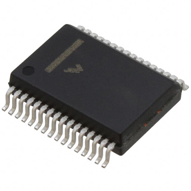
- Part No.:
- MC33993DWB
- Manufacturer:
- NXP Semiconductors
- Category:
- Specialized
- Package:
- 32-BSSOP (0.295", 7.50mm Width)
- Datasheet:
-
 MC33993DWB.pdf
- Description:
- IC INTERFACE SPECIALIZED 32SOIC
- Quantity:
- Payment:

- Shipping:

Inventory:2,436
Please send an inquiry. Send us your inquiry, and we will respond immediately.
Product details
Overview
MC33993DWB from Freescale Semiconductor is a 22-channel multiple switch detection interface IC designed for automotive body control modules. It monitors up to 8 programmable (SP0–SP7) and 14 fixed switch-to-ground (SG0–SG13) inputs, delivers status via SPI, provides analog multiplexing on AMUX, supports 5.5–26 V VPWR operation, and achieves 100 μA typical VPWR standby current in Sleep mode.
For engineers reviewing the MC33993DWB datasheet, MC33993DWB pinout, MC33993DWB application, or MC33993DWB equivalent, this page delivers verified electrical parameters, validated SPI timing constraints, confirmed wetting current options (2.0 mA / 16 mA), real-world switch input voltage range (−14 V to 40 V), and precise thermal shutdown behavior at 155–185 °C.
Technical Context
The MC33993DWB implements dual-mode operation (Normal/Sleep) with hardware-controlled wake-up via WAKE, INT, CS, or switch state change. Its internal architecture integrates a 22-input analog multiplexer, comparator-based switch detection with 4.0 V threshold, programmable wetting current sources/sinks, and SPI interface logic compatible with 3.3 V/5.0 V MCUs at up to 6.0 MHz.
Sleep mode uses a calibrated 64 ms scan timer (±10% accuracy) and draws only 70 μA typical VPWR current; Normal mode enables full register programming-including SP/SG configuration, wake-up/interrupt masking, wetting current selection, and analog channel selection-via 24-bit SPI commands with deterministic interrupt latency (5.0–16 μs).
Key Specifications
| Parameter | Value and Actual Design Meaning |
|---|---|
| Switch Inputs | 22 total: 8 programmable (SP0–SP7), 14 fixed switch-to-ground (SG0–SG13) |
| VPWR Supply Range | 5.5 V to 26 V - supports direct battery connection with reverse-polarity protection required |
| Standby Current (Sleep) | 70 μA typical VPWR current - enables ultra-low-power vehicle keep-alive systems |
| Wetting Current Options | Selectable 2.0 mA or 16 mA per channel - prevents contact oxidation during closure |
| SPI Interface | 24-bit command/response, 3.3 V/5.0 V compatible, up to 6.0 MHz - no level-shifting needed |
| Switch Input Voltage | −14 V to 40 V - withstands load dump, jump-start, and negative transients |
| Thermal Shutdown | 155–185 °C trip point with 5–15 °C hysteresis - protects against sustained overtemperature |
Pinout & Package
Packaged in 32-pin wide-body SOIC (SOICW), footprint code DW, Pb-free (EW suffix), 1.27 mm pitch, 20.0 mm × 7.5 mm body size.
| Pin/Terminal | Circuit Role | Design Meaning |
|---|---|---|
| GND (Pin 1) | Common reference | Shared ground for logic, analog, and switch-to-battery inputs - must be low-impedance |
| SI (Pin 2) | SPI data input | Accepts 24-bit command words from MCU on falling SCLK edge - latches on CS fall |
| SCLK (Pin 3) | SPI clock input | Drives internal shift register - SI sampled on falling edge, SO updated on rising edge |
| CS (Pin 4) | SPI chip select | Active-low enable - falling edge latches switch states and enables SO; rising edge disables SO and clears INT |
| SP0–SP7 (Pins 5–8, 25–28) | Programmable switch inputs | Configurable as switch-to-battery or switch-to-ground - each compared to 4.0 V reference |
| SG0–SG13 (Pins 9–15, 18–24) | Fixed switch-to-ground inputs | Dedicated ground-referenced inputs - closed when voltage < 4.0 V, open when > 4.0 V |
| VPWR (Pin 16) | Battery supply | Main power source for wetting/sustain currents and internal logic - requires external reverse-battery protection |
| WAKE (Pin 17) | Open-drain wake output | Pulled high internally to +5 V in Sleep mode - falling edge wakes device or controls external regulator enable |
| INT (Pin 29) | Open-drain interrupt | Asserted low on enabled switch state change - internal 15–100 μA pull-up to VDD |
| AMUX (Pin 30) | Analog multiplexer output | Buffered analog output of selected SP/SG channel - ±2.5 mV offset, 250 μA drive capability |
| VDD (Pin 31) | Digital supply | 3.3 V/5.0 V logic rail - sets SPI I/O levels and powers SO driver, CS/INT pull-ups |
| SO (Pin 32) | SPI data output | Tri-state until CS falls - outputs 24-bit status word MSB-first with switch states, INT flag, thermal flag |
Key Features
| Feature | Design Value |
|---|---|
| 22-switch monitoring with analog mux | Reduces BOM count by replacing discrete comparators, resistors, and mux ICs in body control units |
| Selectable wetting current (2.0/16 mA) | Enables reliable detection of high-resistance switches (e.g., door latch, hood sensor) without contact degradation |
| Calibrated 64 ms sleep scan timer | Guarantees consistent wake-up latency across temperature and supply voltage - ±10% accuracy |
| −14 V to 40 V switch input tolerance | Eliminates need for external clamping diodes in 12 V/24 V automotive environments |
| Open-drain WAKE and INT outputs | Allows wired-OR connection of multiple MC33993DWB devices to single MCU interrupt line |
Applications
| Door Module Control | Seat Position Sensing |
|---|---|
Use Scenario: Monitoring 12+ mechanical switches (door ajar, lock/unlock, window up/down) in a vehicle door module under 12 V battery supply with transient immunity. IC Role / Device Role / Timing Role: MC33993DWB acts as centralized switch interface - detects closures via 16 mA wetting current, reports status via SPI, and asserts INT to wake MCU from low-power state. Use Value: Reduces PCB area vs. discrete solutions, eliminates false triggers from ESD due to −14 V to 40 V input tolerance, and extends battery life with 70 μA Sleep mode current. | Use Scenario: Reading position feedback from 8 potentiometric seat adjustment switches and 4 limit switches in automotive seating systems. IC Role / Device Role / Timing Role: MC33993DWB configures SP0–SP7 as analog inputs, routes selected channel to AMUX pin, and synchronizes sampling with MCU SPI read cycles. Use Value: Enables analog sensing without dedicated ADC channels on MCU; maintains ±2.5 mV offset accuracy for precise position resolution. |
| Roof Module Switch Interface | Trunk/Liftgate Latch Monitoring |
Use Scenario: Detecting sunroof open/close, tilt, and wind deflector position using 6 SP inputs and 4 SG inputs in a thermally stressed roof console. IC Role / Device Role / Timing Role: MC33993DWB operates in Normal mode during vehicle ON, then enters Sleep mode with 64 ms scan interval when ignition OFF to monitor for forced entry. Use Value: Thermal shutdown (155–185 °C) prevents latch-up during prolonged sun exposure; 100 μA VPWR standby ensures 30-day battery survival. | Use Scenario: Monitoring trunk release, safety interlock, and liftgate position switches in rear cargo systems exposed to moisture and vibration. IC Role / Device Role / Timing Role: MC33993DWB applies 2.0 mA sustain current after initial 16 mA wetting pulse to minimize power draw while maintaining contact integrity. Use Value: Prevents oxide buildup on infrequently actuated latches; −14 V tolerance handles grounding faults during service. |
Equivalent & Alternatives
The following parts are listed as comparable options for similar switch detection interface applications.
| Alternative Part | Technical Difference | Application Difference | Selection Advice |
|---|---|---|---|
| NXP MC33993DWB | Same die, identical pinout and functionality - NXP acquired Freescale in 2015; this is the direct successor part | No functional difference; qualified for same AEC-Q100 Grade 1 (-40°C to 125°C) automotive use cases | Select when sourcing from post-acquisition NXP distribution channels or requiring latest lifecycle support |
| STMicroelectronics VNQ5E04K-E | 8-channel high-side switch with integrated diagnostics - lacks analog mux, SPI interface, and multi-channel wake-up capability | Used for driving loads (e.g., solenoids), not passive switch sensing; requires external MCU polling | Choose only if system needs active switching + basic fault reporting, not 22-channel detection with low-quiescent sleep |
Compared with NXP MC33993DWB, the original Freescale MC33993DWB shares identical electrical specs and package but may have older date codes and limited long-term availability; versus VNQ5E04K-E, MC33993DWB provides 2.75× more inputs, integrated SPI, analog multiplexing, and 10× lower sleep current - making it irreplaceable for complex body electronics architectures.
Availability
MC33993DWB is available at Aetrix Electronics and suitable for automotive body control modules, industrial HMI panels, and commercial vehicle telematics systems requiring stable component supply across extended temperature ranges and long production lifecycles.
Supply support for MC33993DWB includes scheduled delivery planning, volume procurement assistance, BOM continuity management, traceable sourcing, and lifecycle availability coordination for OEM customers, industrial embedded developers, connected-device designers, and electronics production programs.
Manufacturer
Freescale Semiconductor was a leading designer of embedded processors and analog/mixed-signal ICs, acquired by NXP Semiconductors in 2015. Its automotive portfolio emphasized robustness, AEC-Q100 qualification, and system-level integration.
The MC33993DWB belongs to Freescale's Body Electronics Interface product line, engineered specifically for centralized switch monitoring in automotive body control units where low quiescent current, high-voltage tolerance, and SPI-based diagnostics are mandatory.
FAQ
What is the maximum VPWR voltage the MC33993DWB can withstand?
The MC33993DWB supports a maximum VPWR voltage of 50 V under absolute maximum ratings, with continuous operation specified from 5.5 V to 26 V. Transient spikes beyond 40 V must be clamped externally. This rating ensures survivability during automotive load-dump events and jump-start conditions without damage to the internal wetting current sources or logic circuitry. The MC33993DWB maintains functional integrity across this full range when used with appropriate external protection.
Does the MC33993DWB support both 3.3 V and 5.0 V microcontrollers?
Yes, the MC33993DWB supports direct interfacing with both 3.3 V and 5.0 V MCUs via its SPI interface. The VDD pin sets the logic levels for SI, SO, SCLK, and CS - SO output high is VDD – 0.8 V minimum, and input thresholds are defined between 0.8 V and 2.2 V. No level-shifting circuitry is required. The MC33993DWB has been production-tested at 4.16 MHz with 5.0 V SPI and operates reliably up to 6.0 MHz, making it compatible with common automotive microcontrollers like S32K and MPC57xx families.
How does the MC33993DWB handle switch debouncing?
MC33993DWB does not implement hardware debouncing; instead, it relies on controlled wetting current timing and MCU firmware. The device provides a 20 ms wetting current pulse (configurable per channel) followed by 2.0 mA sustain current, which inherently suppresses bounce by ensuring clean contact closure before status sampling. Switch state changes are latched on the falling edge of CS, and the MCU reads the stable 24-bit status word. Debounce filtering must be implemented in host software using consecutive SPI reads or timer-based validation - a design choice that preserves flexibility and avoids fixed hardware delays. This behavior is consistent across all MC33993DWB units.
Can the MC33993DWB detect switches connected to battery or ground using the same pins?
Only the SP0–SP7 pins (Pins 5–8, 25–28) on the MC33993DWB are programmable for either switch-to-battery or switch-to-ground configuration via the Settings Command register. The SG0–SG13 pins (Pins 9–15, 18–24) are fixed switch-to-ground inputs only. When configured as switch-to-battery, SPn inputs detect closure when voltage exceeds 4.0 V; as switch-to-ground, they detect closure when voltage falls below 4.0 V. This dual-mode capability allows one MC33993DWB to replace multiple discrete interfaces in mixed topologies - for example, reading both door handle switches (battery-referenced) and seat belt buckles (ground-referenced) simultaneously.
What is the purpose of the AMUX pin on the MC33993DWB?
The AMUX pin on the MC33993DWB is the buffered analog multiplexer output, enabling the device to function as an analog front-end for potentiometers, thermistors, or other resistive sensors. When an SP or SG input is selected via the Analog Command register, its voltage appears on AMUX with ±2.5 mV offset and <30 mV low-state output voltage under 250 μA sink load. This allows the MCU to perform precise ratiometric measurements using its internal ADC without adding external op-amps or mux ICs. The MC33993DWB's AMUX capability directly reduces system BOM cost and board space in applications like seat position sensing or HVAC blend door feedback.
MC33993DWB Specifications
- Product attributes
- Attribute value
- Manufacturer:
- NXP Semiconductors
- Series:
- -
- Package/Case:
- 32-BSSOP (0.295", 7.50mm Width)
- Packaging:
- Tube
- Product Status:
- Obsolete
- Applications:
- -
- Interface:
- SPI Serial
- Voltage - Supply:
- 5.5V ~ 26V
- Supplier Device Package:
- 32-SOIC
- Grade:
- Automotive
- Qualification:
- -
- Mounting Type:
- Surface Mount
MC33993DWB FAQ
1.How can I place an order for MC33993DWB through Aetrix?
Please submit a Request for Quotation (RFQ) for MC33993DWB on Aetrix. Our sales agent will provide a competitive quotation and guide you through the order confirmation once you accept the terms.
2.Are the price and stock information for MC33993DWB reliable?
The price and inventory of MC33993DWB are updated periodically and may fluctuate due to market conditions. Stock and pricing data are typically refreshed every 24 hours. Quotation validity for MC33993DWB is usually 5 days.
3.What payment methods are accepted for MC33993DWB?
We accept Wire Transfer, PayPal, Credit Card, Western Union, MoneyGram, and Escrow for MC33993DWB transactions.
Note: Certain payment methods may incur a processing fee.
4.How is shipping managed for MC33993DWB?
MC33993DWB orders can be shipped via leading logistics carriers, including DHL, UPS, FedEx, TNT, or Registered Mail.
Once your MC33993DWB order is processed, you will receive an email with the shipment details and tracking number.
Note: Tracking information may take up to 24 hours to appear. Express delivery typically takes 3–5 business days.
5.How can I obtain technical support or documentation for MC33993DWB?
For technical support, including MC33993DWB datasheets, pinout diagrams, or application guidance, please contact our engineering support team. They can provide detailed documentation and assistance for your MC33993DWB requirements.
6.How does Aetrix verify that MC33993DWB is sourced from the original manufacturer or authorized distributors?
All MC33993DWB products on Aetrix are procured from qualified distributors and authorized channels. Our dedicated quality assurance team conducts strict verification, including traceability checks and, if necessary, third-party testing. This ensures that MC33993DWB meets industry standards.
7.What is the process for return or replacement of MC33993DWB?
All MC33993DWB units undergo pre-shipment inspection (PSI). If there is an issue with MC33993DWB, returns or replacements are accepted under the following conditions:
1.Quantity discrepancies, incorrect items, or visible external defects (such as breakage or corrosion), acknowledged by Aetrix.
2.The issue is reported within 90 days of delivery.
3.The MC33993DWB part is unused and in its original packaging.
Return procedure for MC33993DWB:
1.Submit a request within 90 days.
2.Obtain a Return Material Authorization (RMA) from Aetrix.
MC33993DWB Tags

-
NVT4857UKAZ
NXP Semiconductors

-
TCA8418RTWR
Texas Instruments

-
PCA9546APWR
Texas Instruments

-
MD0100N8-G
Microchip Technology

-
PCA9548APW,118
NXP Semiconductors

-
PCA9540BDP,118
NXP Semiconductors

-
PCA9548APWR
Texas Instruments

-
PCA9546APW,118
NXP Semiconductors

-
PTN3360DBS,518
NXP Semiconductors

-
PCA9546ABS,118
NXP Semiconductors

-
PCA9518PWR
Texas Instruments

-
PCA9545APW,118
NXP Semiconductors
Tech Hub

A practical engineering guide to 3.3V and 5V logic compatibility, input thresholds, resistor dividers, translator ICs, MOSFET level shifting, I2C pull-ups, timing limits and power-sequencing risks.

The 74HC595 uses push-pull logic outputs, while the TPIC6B595 uses 50 V open-drain DMOS sinks for higher-power loads. This guide compares timing, current limits, 3.3 V interfacing, load wiring, thermal…

The 74HC595 converts serial data into eight stable parallel outputs. This guide covers pin functions, shift and storage timing, OE and MR behavior, drive-current limits, cascading, voltage compatibilit…

A technical comparison of level-sensitive latches and edge-triggered flip-flops, covering timing windows, setup and hold limits, master–slave operation, time borrowing, race-through, HDL inference and…

A D latch stores one bit while Enable controls when data can pass. This reference covers gate-level operation, truth tables, transparency, setup and hold timing, LE versus OE, common ICs and practical …

An SR latch stores one bit through cross-coupled feedback. This engineering reference covers NOR and NAND implementations, truth tables, forbidden-state recovery, gated operation, switch debouncing, fa…

Latch circuits retain one bit through feedback. This technical reference covers SR and D latches, truth tables, transparency, timing limits, latch-versus-flip-flop behavior, applications and common log…

An engineering guide to LED driver operation, constant-current and constant-voltage outputs, linear and switching topologies, dimming, IC selection, calculations, replacement compatibility, and fault c…

Operational amplifier guide covering op amp basics, feedback, ideal vs real op amps, common configurations, buffer circuits, offset, bias current, gain-bandwidth, slew rate, rail-to-rail limits and sel…

Jumper cables guide covering safe connection order, red and black clamp placement, final ground connection, cable gauge, length, clamp quality, copper vs CCA cables, jump starter comparison and battery…


