
 My Inquiry
 My Account


NXP Semiconductors MC34118DW
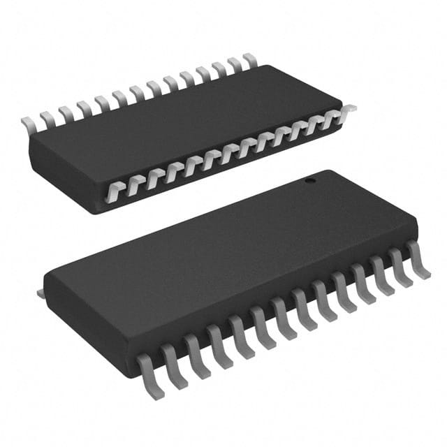
- Part No.:
- MC34118DW
- Manufacturer:
- NXP Semiconductors
- Category:
- Telecom
- Package:
- 28-SOIC (0.295", 7.50mm Width)
- Datasheet:
-
 MC34118DW.pdf
- Description:
- IC TELECOM INTERFACE 28SOIC
- Quantity:
- Payment:

- Shipping:

Inventory:2,346
Please send an inquiry. Send us your inquiry, and we will respond immediately.
Product details
Overview
MC34118DW from ON Semiconductor (formerly Motorola) is a voice-switched speakerphone circuit IC designed for hands-free telephony systems. It integrates microphone amplifier with mute, complementary transmit/receive attenuators (52 dB range), background noise monitors for both paths, dial tone detector, hybrid amplifiers, and chip disable - all operating from 3.0–6.5 V on-loop or supply power. Used in standalone speakerphones interfacing directly to Tip/Ring via coupling transformer.
For engineers reviewing the MC34118DW datasheet, MC34118DW pinout, MC34118DW application, or MC34118DW equivalent, key selection criteria include its line-powered operation (5.0 mA typical), 28-pin SOICW package (DW suffix), Pb-free EG variant compliance, CT-controlled mode switching timing, and dual-level detection architecture for robust half-duplex control in noisy environments.
Technical Context
The MC34118DW implements a fully analog, comparator-based voice activity detection system with four independent level detectors (TLI1/RLI1/TLI2/RLI2), two background noise monitors (CPT/CPR), and an AGC circuit that reduces receive gain by ≈25 dB when VCC drops below 3.5 V. Its attenuator control block produces a single CT voltage (±240 mV vs VB) to drive complementary +6 dB/–46 dB transmit and receive paths while maintaining constant sum gain (–40 dB ±0.1 dB).
It features two hybrid amplifiers (HTI→HTO– with external gain setting; HTO–→HTO+ with fixed –1.0 gain) for transformer-coupled 2-wire to 4-wire conversion, plus a high-impedance filter input (FI >1.0 MΩ) and low-impedance filter output (FO <50 Ω) for user-defined 60 Hz rejection or other signal conditioning. All internal biasing references VB ≈ VCC/2.
Key Specifications
| Parameter | Value and Actual Design Meaning |
|---|---|
| Supply Voltage Range | 3.0–6.5 V DC - supports direct telephone line powering (≈5.0 mA typical) or local supply |
| Attenuator Gain Range | 52 dB - full dynamic range between Tx max gain (+6 dB) and Rx max attenuation (–46 dB) |
| Operating Temperature | –20°C to +60°C - qualified for commercial-grade telephony equipment deployment |
| Package Type | 28-pin SOICW (Case 751F) - surface-mount compatible with Pb-free EG suffix |
| CT Control Voltage Range | ±240 mV vs VB - directly sets attenuator mode: +240 mV = Rx, –240 mV = Tx, 0 V = idle |
| Input Signal Limit | 350 mVRMS at TXI/RXI - prevents distortion; clamped input stage enforces safe swing |
| Volume Control Range | 27–35 dB - adjustable via VLC pin (0.3×VB to VB); affects only receive path gain |
Pinout & Package
MC34118DW uses a 28-pin SOICW (Small Outline Integrated Circuit, Wide-body) package per Case 751F, identical pinout to the PDIP version. Pin numbering is top-view, counterclockwise from notch.
| Pin/Terminal | Circuit Role | Design Meaning |
|---|---|---|
| 1 FO | Filter Output | Low-impedance (<50 Ω) buffered output for external high-pass or bandpass filtering |
| 2 FI | Filter Input | High-impedance (>1.0 MΩ) node for injecting filtered receive signal before RXI |
| 3 CD | Chip Disable | Logic-low (<0.8 V) enables operation; logic-high (>2.0 V) powers down entire IC to conserve loop current |
| 4 VCC | Main Supply | Accepts 3.0–6.5 V; draws 5.5 mA typical at 6.5 V, 600 µA in disabled state |
| 5 HTO+ | Hybrid Amp Output (+) | Differential output (with HTO–) to transformer primary; fixed –1.0 gain |
| 6 HTO– | Hybrid Amp Output (–) | Differential output (with HTO+) to transformer primary; gain set by external R at HTI |
| 7 HTI | Hybrid Amp Input | Summing node biased at VB; connects to transformer secondary for 2-wire interface |
| 8 TXO | Transmit Attenuator Output | DC level ≈VB; drives HTO–/HTO+; output impedance <10 Ω until current limit (~2.5 mA) |
| 9 TXI | Transmit Attenuator Input | 10 kΩ input impedance; accepts up to 350 mVRMS from microphone amp (MCO) |
| 10 MCO | Microphone Amp Output | Gain set by external resistors; open-loop gain 80 dB; output swing ≤VCC–1.0 V |
| 11 MCI | Microphone Amp Input | Summing node biased at VB; accepts mic signal referenced to VB |
| 12 MUT | Mute Control | Logic-low enables mic amp; logic-high (>2.0 V) reduces gain by ≥55 dB without disabling rest of IC |
| 13 VLC | Volume Control Input | Analog voltage (0.3×VB to VB) controlling receive attenuator gain only; 60 nA sink current |
| 14 CT | Attenuator Control | Drives external RC network; ±240 mV vs VB selects Tx/Rx/idle mode; ±60 µA sourcing/sinking |
| 15 VB | Bias Reference | Internal ≈VCC/2 output; used as AC ground and bias for VLC, CT, and amplifier nodes; requires ≥220 µF capacitor |
| 16 CPT | Transmit Noise Monitor RC | External RC sets time constant (~4.7 s) for transmit background noise tracking |
| 17 TLI2 | Transmit Level Detector 2 Input | Monitors mic/speaker side signal level; paired with TLO2 to detect speech bursts |
| 18 TLO2 | Transmit Level Detector 2 Output | Charges external cap; feeds comparator in control block; fast rise/slow decay |
| 19 RLO2 | Receive Level Detector 2 Output | Monitors speaker amp output side; paired with RLI2; same timing behavior as TLO2 |
| 20 RLI2 | Receive Level Detector 2 Input | Connects to speaker amp output (e.g., MC34119); detects local acoustic feedback |
| 21 RXI | Receive Attenuator Input | 10 kΩ input; accepts up to 350 mVRMS from line (Tip/Ring via transformer); feeds dial tone detector |
| 22 RXO | Receive Attenuator Output | DC level ≈VB; drives speaker amplifier; output impedance <10 Ω until current limit |
| 23 TLI1 | Transmit Level Detector 1 Input | Monitors hybrid output (line side); paired with TLO1 to detect far-end speech |
| 24 TLO1 | Transmit Level Detector 1 Output | Feeds comparator with RLO1; enables cross-path talk detection |
| 25 RLO1 | Receive Level Detector 1 Output | Monitors Tip/Ring input; paired with RLI1; provides line-side speech detection |
| 26 RLI1 | Receive Level Detector 1 Input | Connects directly to transformer secondary (Tip/Ring side); detects near-end speech |
| 27 CPR | Receive Noise Monitor RC | External RC sets ~4.7 s time constant for receive background noise tracking |
| 28 GND | Ground Reference | System ground return for all internal circuits; separate from VB reference plane |
Key Features
| Feature | Design Value |
|---|---|
| Dual Background Noise Monitors | Independent CPT/CPR RC networks reject steady-state room/line noise while preserving speech burst detection |
| Dial Tone Detector | 15 mV threshold comparator disables receive idle mode during dial tone, preventing attenuation of signaling tones |
| Line-Power Optimized AGC | Reduces receive gain by ≈25 dB when VCC falls below 3.5 V - maintains stability on long telephone loops |
| Chip Disable (CD) Pin | Reduces quiescent current to 600 µA - enables low-power standby in battery-backed or loop-limited systems |
| Hybrid Amplifier Pair | HTI→HTO– (externally gain-set) + HTO–→HTO+ (fixed –1.0) form complete 2-to-4 wire converter with transformer |
| 4-Point Signal Sensing | TLI1/RLI1 (line side) + TLI2/RLI2 (speaker/mic side) enable robust full-system voice activity discrimination |
Applications
| Conference Speakerphone | Hotel/Motel Room Phone |
|---|---|
Use Scenario: Wall-mounted hands-free unit in meeting rooms with ambient noise up to 55 dBA. IC Role / Device Role / Timing Role: Core voice-switching engine performing real-time Tx/Rx path selection, background noise suppression, and hybrid interfacing to POTS line. Use Value: Enables full-duplex illusion via 30 ms fast-idle switching and 1 s slow-idle recovery - eliminates echo without DSP hardware. |
Use Scenario: Feature-rich analog room phone supporting speaker mode, mute, and volume control. IC Role / Device Role / Timing Role: Integrates microphone preamp, speaker driver interface, and line-side signal conditioning in single IC. Use Value: Reduces BOM count by replacing discrete op-amps, comparators, and attenuator networks - simplifies layout and calibration. |
| Public Kiosk Telephone | Emergency Call Station |
Use Scenario: Outdoor kiosk exposed to traffic noise, wind, and variable handset usage patterns. IC Role / Device Role / Timing Role: Provides adaptive gain control, dial-tone preservation, and chip-disable for power cycling between calls. Use Value: Maintains intelligibility under 70 dBA broadband noise using dual-path background monitors and 4-point sensing. |
Use Scenario: Life-safety station requiring fail-safe operation, low standby current, and immunity to false triggering. IC Role / Device Role / Timing Role: Delivers deterministic half-duplex control with AGC fallback at low loop voltage and hardwired mute override. Use Value: Guarantees call initiation even at 2.8 V VCC via AGC-assisted gain management - meets UL/EN60950 reliability thresholds. |
Equivalent & Alternatives
The following parts are listed as comparable options for similar voice-switched speakerphone applications.
| Alternative Part | Technical Difference | Application Difference | Selection Advice |
|---|---|---|---|
| MC34119P | Speaker amplifier companion IC; lacks attenuators, level detectors, and CT control - requires MC34118DW for full speakerphone function | Only suitable as RXO load driver; cannot replace MC34118DW's core switching logic or hybrid interface | Select MC34119P only when augmenting MC34118DW with higher-power speaker drive capability. |
| NJR NJM2118M | Functionally similar speakerphone IC but uses different CT voltage polarity and lacks integrated dial tone detector; 24-pin SSOP package | Requires redesign of RC timing network and external dial tone handling; not drop-in compatible | Choose NJM2118M only for new designs where footprint change and timing recalibration are acceptable. |
Compared with MC34119P (amplifier-only) and NJM2118M (alternate architecture), the MC34118DW delivers complete analog speakerphone functionality in one 28-pin SOICW device - including line-powered operation, deterministic mode switching, and transformer-coupled hybrid interface - making it uniquely suited for cost-sensitive, space-constrained POTS endpoints.
Availability
MC34118DW is available at Aetrix Electronics and suitable for conference speakerphones, hotel room phones, public kiosks, and emergency call stations requiring stable component supply across extended product lifecycles.
Supply support for MC34118DW includes scheduled delivery planning, volume procurement assistance, BOM continuity management, traceable sourcing, and lifecycle availability coordination for OEM customers, industrial embedded developers, connected-device designers, and electronics production programs.
Manufacturer
ON Semiconductor (acquired Motorola's semiconductor business in 2004) is a global supplier of energy-efficient silicon solutions for automotive, industrial, cloud, and communications markets.
The MC34118DW belongs to ON Semiconductor's legacy telephony analog IC portfolio, engineered specifically for reliable, low-cost, no-DSP speakerphone implementation in analog telephone interfaces and feature phones.
FAQ
What is the minimum supply voltage required for stable operation of the MC34118DW?
The MC34118DW operates reliably from 3.0 V to 6.5 V. Below 3.5 V, its internal AGC circuit reduces receive attenuator gain by up to 25 dB to maintain stability on long telephone loops - ensuring continuous functionality even at 2.8 V, though with reduced audio output level. This behavior is fully characterized in the Recommended Operating Limits table of the MC34118DW datasheet.
How does the MC34118DW handle dial tones to prevent unintended attenuation?
The MC34118DW includes a dedicated dial tone detector with a 15 mV threshold comparator referenced to VB. When active in receive mode and an incoming signal exceeds this level - such as standard 350 Hz/440 Hz dial tones - the detector disables receive idle mode, locking the receive attenuator at volume-controlled gain. This ensures consistent loudness of signaling tones, preventing fade-out during number entry. The function is intrinsic to the MC34118DW design and requires no external components.
Can the MC34118DW be powered directly from the telephone line, and what current does it draw?
Yes, the MC34118DW is explicitly designed for line-powered operation, drawing approximately 5.0 mA typical from the telephone loop at 6.5 V. Its low-voltage operation (down to 3.0 V) and Chip Disable (CD) pin - reducing current to 600 µA - make it ideal for loop-powered speakerphones. The MC34118DW datasheet specifies ICC = 5.5 mA max at VCC = 6.5 V and CD ≤ 0.8 V, confirming compatibility with standard POTS line constraints.
What is the purpose of the VB pin on the MC34118DW, and how must it be decoupled?
The VB pin on the MC34118DW outputs a stable ≈VCC/2 bias voltage used as AC ground and reference for all internal amplifiers, attenuators, and level detectors. It must be decoupled with a minimum 220 µF low-ESR capacitor to GND to suppress ripple and ensure stable mode switching. Failure to adequately bypass VB causes erratic CT voltage transitions and degraded noise rejection - a critical requirement explicitly called out in the MC34118DW application notes and functional description.
Does the MC34118DW support differential hybrid interfacing, and which pins are involved?
Yes, the MC34118DW supports transformer-coupled differential hybrid interfacing via pins HTI (hybrid input), HTO– (first hybrid amp output), and HTO+ (second hybrid amp output). HTI accepts the transformer secondary signal; HTO– gain is set externally; HTO+ provides fixed –1.0 gain to complete the balanced 2-wire to 4-wire conversion. This architecture is integral to the MC34118DW's ability to reject common-mode line noise and enable full-duplex-capable speakerphone operation.
MC34118DW Specifications
- Product attributes
- Attribute value
- Manufacturer:
- NXP Semiconductors
- Series:
- -
- Package/Case:
- 28-SOIC (0.295", 7.50mm Width)
- Packaging:
- Tube
- Product Status:
- Obsolete
- Function:
- Voice-Switched Speakerphone
- Interface:
- -
- Number of Circuits:
- 1
- Voltage - Supply:
- 3.5V ~ 6.5V
- Current - Supply:
- 5.5mA
- Power (Watts):
- -
- Operating Temperature:
- -20°C ~ 60°C
- Grade:
- -
- Qualification:
- -
- Mounting Type:
- Surface Mount
- Supplier Device Package:
- 28-SOIC
MC34118DW FAQ
1.How can I place an order for MC34118DW through Aetrix?
Please submit a Request for Quotation (RFQ) for MC34118DW on Aetrix. Our sales agent will provide a competitive quotation and guide you through the order confirmation once you accept the terms.
2.Are the price and stock information for MC34118DW reliable?
The price and inventory of MC34118DW are updated periodically and may fluctuate due to market conditions. Stock and pricing data are typically refreshed every 24 hours. Quotation validity for MC34118DW is usually 5 days.
3.What payment methods are accepted for MC34118DW?
We accept Wire Transfer, PayPal, Credit Card, Western Union, MoneyGram, and Escrow for MC34118DW transactions.
Note: Certain payment methods may incur a processing fee.
4.How is shipping managed for MC34118DW?
MC34118DW orders can be shipped via leading logistics carriers, including DHL, UPS, FedEx, TNT, or Registered Mail.
Once your MC34118DW order is processed, you will receive an email with the shipment details and tracking number.
Note: Tracking information may take up to 24 hours to appear. Express delivery typically takes 3–5 business days.
5.How can I obtain technical support or documentation for MC34118DW?
For technical support, including MC34118DW datasheets, pinout diagrams, or application guidance, please contact our engineering support team. They can provide detailed documentation and assistance for your MC34118DW requirements.
6.How does Aetrix verify that MC34118DW is sourced from the original manufacturer or authorized distributors?
All MC34118DW products on Aetrix are procured from qualified distributors and authorized channels. Our dedicated quality assurance team conducts strict verification, including traceability checks and, if necessary, third-party testing. This ensures that MC34118DW meets industry standards.
7.What is the process for return or replacement of MC34118DW?
All MC34118DW units undergo pre-shipment inspection (PSI). If there is an issue with MC34118DW, returns or replacements are accepted under the following conditions:
1.Quantity discrepancies, incorrect items, or visible external defects (such as breakage or corrosion), acknowledged by Aetrix.
2.The issue is reported within 90 days of delivery.
3.The MC34118DW part is unused and in its original packaging.
Return procedure for MC34118DW:
1.Submit a request within 90 days.
2.Obtain a Return Material Authorization (RMA) from Aetrix.
MC34118DW Tags

-
LMC567CMX/NOPB
Texas Instruments
-
LM567CMX/NOPB
Texas Instruments
-
LM567CM/NOPB
Texas Instruments

-
VSC8531XMW-02
Microchip Technology
-
VSC8531XMW-05
Microchip Technology

-
GPY115C0VI
MaxLinear, Inc.

-
SI32185-A-FMR
Skyworks Solutions Inc.

-
VSC8541XMV-05
Microchip Technology

-
SI32178-B-FM1R
Skyworks Solutions Inc.
-
GPY215C0VI
MaxLinear, Inc.

-
CPC7514ZTR
Littelfuse Inc.

-
VSC8502XML-03
Microchip Technology
Tech Hub

A practical engineering guide to 3.3V and 5V logic compatibility, input thresholds, resistor dividers, translator ICs, MOSFET level shifting, I2C pull-ups, timing limits and power-sequencing risks.

The 74HC595 uses push-pull logic outputs, while the TPIC6B595 uses 50 V open-drain DMOS sinks for higher-power loads. This guide compares timing, current limits, 3.3 V interfacing, load wiring, thermal…

The 74HC595 converts serial data into eight stable parallel outputs. This guide covers pin functions, shift and storage timing, OE and MR behavior, drive-current limits, cascading, voltage compatibilit…

A technical comparison of level-sensitive latches and edge-triggered flip-flops, covering timing windows, setup and hold limits, master–slave operation, time borrowing, race-through, HDL inference and…

A D latch stores one bit while Enable controls when data can pass. This reference covers gate-level operation, truth tables, transparency, setup and hold timing, LE versus OE, common ICs and practical …

An SR latch stores one bit through cross-coupled feedback. This engineering reference covers NOR and NAND implementations, truth tables, forbidden-state recovery, gated operation, switch debouncing, fa…

Latch circuits retain one bit through feedback. This technical reference covers SR and D latches, truth tables, transparency, timing limits, latch-versus-flip-flop behavior, applications and common log…

An engineering guide to LED driver operation, constant-current and constant-voltage outputs, linear and switching topologies, dimming, IC selection, calculations, replacement compatibility, and fault c…

Operational amplifier guide covering op amp basics, feedback, ideal vs real op amps, common configurations, buffer circuits, offset, bias current, gain-bandwidth, slew rate, rail-to-rail limits and sel…

Jumper cables guide covering safe connection order, red and black clamp placement, final ground connection, cable gauge, length, clamp quality, copper vs CCA cables, jump starter comparison and battery…


