
 My Inquiry
 My Account


NXP Semiconductors MC34GD3000EP
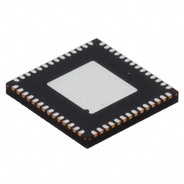
- Part No.:
- MC34GD3000EP
- Manufacturer:
- NXP Semiconductors
- Category:
- Motor Drivers, Controllers
- Package:
- 56-VFQFN Exposed Pad
- Datasheet:
-
 MC34GD3000EP.pdf
- Description:
- GD3000 - Brushless DC Motor Gate
- Quantity:
- Payment:

- Shipping:

Inventory:188
Please send an inquiry. Send us your inquiry, and we will respond immediately.
Product details
Overview
MC34GD3000EP from NXP Semiconductors is a three-phase FET predriver IC for automotive motor control, integrating six gate drivers (three high-side and three low-side), programmable dead time via SPI, 15 V regulated VLS supply, and integrated current-sensing amplifier. It operates from 6.0 V to 60 V input, delivers up to 2.5 A peak gate drive, and is AEC-Q100 Grade 1 qualified for engine bay applications including electric power steering and belt starter generators.
For engineers reviewing the MC34GD3000EP datasheet, MC34GD3000EP pinout, MC34GD3000EP application, or MC34GD3000EP equivalent, key selection criteria include bootstrap-capable high-side drive architecture, SPI-configurable protection thresholds, 56-pin HVQFN thermal-enhanced package with exposed pad, and compatibility with 12 V/48 V automotive systems requiring robust overcurrent and desaturation detection.
Technical Context
The MC34GD3000EP implements a dual-regulator architecture: VDD (5.0 V) powers logic and SPI interface, while VLS (15 V) supplies gate drives and bootstrap circuits. Its six independent gate outputs support external N-channel MOSFETs in three-phase bridge configurations, with each high-side driver relying on discrete bootstrap capacitors referenced to phase-specific HS source pins (e.g., PA_HS_S).
Functional safety features include asynchronous EN1/EN2 enable logic requiring both signals high to activate outputs, hardware reset (RST_B), interrupt reporting (INT), and configurable overcurrent detection using AMP_P/AMP_N inputs and OC_TH threshold setting. The SPI port (3.0 MHz max, MSB-first) enables runtime configuration of dead time, fault masking, and initialization sequencing.
Key Specifications
| Parameter | Value and Actual Design Meaning |
|---|---|
| Supply Range | 6.0 V to 60 V VPWR - supports 12 V and 48 V automotive battery systems with load-dump survival up to 80 V |
| Gate Drive Current | 1.0 A to 2.5 A peak - sufficient to charge >400 nC gate capacitance of low-RDS(on) power FETs |
| VLS Output Voltage | 13.5 V to 17 V - regulated 15 V supply for low-side drivers and bootstrap circuitry, stable across 8–40 V VPWR |
| SPI Interface Speed | Up to 5.0 MHz - enables real-time dead time adjustment and fault register polling in fast-control-loop systems |
| AEC-Q100 Grade | Grade 1 (–40 °C to +125 °C ambient) - qualified for under-hood automotive applications including EPS and cooling fans |
| Thermal Resistance | RθJC = 3.0 °C/W - enables high-power operation with proper heatsinking via exposed pad (EP) |
| Bootstrap Voltage | 22 V to 32 V at VSUP = 14 V - ensures reliable high-side FET turn-on even during battery sag |
Pinout & Package
HVQFN56 (SOT684-17): 8 mm × 8 mm × 0.9 mm body, 0.5 mm pitch, thermal-enhanced plastic quad flatpack with exposed pad (EP) for PCB-level heat dissipation. Pin 55 (PA_HS_S) serves as primary thermal reference point per RθJC specification.
| Pin/Terminal | Circuit Role | Design Meaning |
|---|---|---|
| PA_HS_G, PB_HS_G, PC_HS_G | High-side gate drive outputs | Low-impedance totem-pole drivers limiting gate voltage to ~15 V above respective HS source (e.g., PA_HS_S); resist negative current injection |
| PA_LS_G, PB_LS_G, PC_LS_G | Low-side gate drive outputs | 15 V capable outputs referenced to VSS; designed for direct connection to low-side FET gates without level shifting |
| PA_BOOT, PB_BOOT, PC_BOOT | Bootstrap capacitor inputs | Analog inputs accepting external capacitors (10–20× FET Ciss) to generate floating 15 V bias for high-side drivers |
| EN1, EN2 | Enable logic inputs | Asynchronous AND-gated enables - both must be high to activate any gate output; prevents shoot-through during startup |
| AMP_P, AMP_N, OC_TH | Current sense interface | Differential amplifier inputs (±7 V range) and programmable overcurrent threshold input enabling precise shunt-based motor phase current monitoring |
Key Features
| Feature | Design Value |
|---|---|
| Programmable dead time | SPI-configurable blanking interval prevents simultaneous conduction in half-bridge legs, critical for IGBT/MOSFET short-circuit avoidance |
| Integrated VLS regulator | 15 V linear regulator (600 mA typical peak) eliminates need for external high-current LDO, reducing BOM count and PCB area |
| Trickle charge pump | On-chip charge pump maintains bootstrap voltage during extended low-duty-cycle operation, enabling continuous high-side drive in fan/pump applications |
| Desaturation detection | VSUP-referenced comparator monitors phase voltage collapse during overcurrent events, providing fast (<1 µs) fault response independent of shunt sensing |
| Safe SPI initialization | Dedicated command sequence ensures controlled startup: LS drivers pulse before HS drivers, guaranteeing bootstrap capacitor charging prior to high-side activation |
Applications
| Electric Power Steering (EPS) | Cooling Fan Control |
|---|---|
Use Scenario: Closed-loop torque assist in 12 V or 48 V vehicle architectures with rapid transient response requirements. IC Role / Device Role / Timing Role: Three-phase predriver interfaces MCU PWM commands to external 4 mΩ Si MOSFETs, managing gate timing, dead time, and overcurrent shutdown. Use Value: Integrated desaturation detection and programmable dead time reduce system-level fault latency below 2 µs, meeting ISO 26262 ASIL-B timing constraints. | Use Scenario: Variable-speed radiator fan driven by 12 V battery with PWM-controlled airflow and thermal derating. IC Role / Device Role / Timing Role: Pre-driver provides high-current gate drive (2.5 A peak) to low-RDS(on) N-channel FETs while monitoring phase current via integrated amplifier. Use Value: Trickle charge pump sustains high-side drive during 5–10 % duty cycle operation, eliminating external boost circuitry and improving efficiency by >3 % at low speed. |
| Water Pump Actuation | Belt Starter Generator (BSG) |
Use Scenario: High-reliability coolant circulation in hybrid powertrains with frequent start-stop cycles and wide temperature range. IC Role / Device Role / Timing Role: Controls three-phase inverter driving brushless DC water pump motor; uses SPI to adapt dead time based on battery voltage and temperature. Use Value: AEC-Q100 Grade 1 qualification and –40 °C to +125 °C operation ensure uninterrupted function during cold cranking and under-hood thermal stress. | Use Scenario: 48 V mild-hybrid BSG system requiring bidirectional energy flow, regenerative braking, and engine restart capability. IC Role / Device Role / Timing Role: Pre-driver manages synchronous rectification and commutation timing for high-efficiency motor/generator operation with <100 ns propagation delay. Use Value: Dual enable (EN1/EN2) logic and hardware reset (RST_B) enable fail-safe shutdown within 77 ns, satisfying functional safety requirements for torque interruption. |
Equivalent & Alternatives
The following parts are listed as comparable options for similar three-phase gate driver applications.
| Alternative Part | Technical Difference | Application Difference | Selection Advice |
|---|---|---|---|
| MC33GD3000AEP | Same pinout and electrical specs; differs only in traceability marking and packaging (tape-and-reel vs. tray) | No functional difference; identical use in EPS, pumps, and fans | Select MC33GD3000AEP for automated SMT assembly requiring standard tape-and-reel delivery |
| MPQ6532-AEC1 | Monolithic 3-phase driver (no external FETs); integrates 60 V/2.5 A half-bridges; lacks SPI configurability and desat detection | Suitable for space-constrained designs where integration outweighs programmability needs | Choose MPQ6532-AEC1 when board area is critical and fixed dead time suffices; not drop-in for MC34GD3000EP due to different topology |
Compared with MC34GD3000EP, MC33GD3000AEP offers identical performance in a different packaging format, while MPQ6532-AEC1 trades SPI flexibility and fault diagnostics for higher integration-making it viable only where monolithic drive and smaller footprint justify loss of configurability and enhanced protection features.
Availability
MC34GD3000EP is available at Aetrix Electronics and suitable for automotive motor control, electric power steering, and cooling fan applications requiring stable component supply across long production lifecycles.
Supply support for MC34GD3000EP includes scheduled delivery planning, volume procurement assistance, BOM continuity management, traceable sourcing, and lifecycle availability coordination for OEM customers, industrial embedded developers, connected-device designers, and electronics production programs.
Manufacturer
NXP Semiconductors is a global semiconductor company headquartered in Eindhoven, Netherlands, specializing in secure connectivity solutions for automotive, industrial, and IoT markets.
The MC34GD3000EP belongs to NXP's GD3000 family of high-voltage gate drivers, engineered specifically for AEC-Q100-compliant three-phase motor control in demanding automotive environments such as EPS, water pumps, and BSG systems.
FAQ
What is the maximum bootstrap capacitor voltage rating supported by the MC34GD3000EP?
The MC34GD3000EP limits bootstrap capacitor voltage to approximately 15 V, as specified in the absolute maximum ratings table for VBOOT. This constraint applies to all three bootstrap inputs (PA_BOOT, PB_BOOT, PC_BOOT) and ensures safe gate bias generation for high-side FETs without exceeding internal clamp thresholds. Exceeding 15 V risks damaging internal bootstrap diodes or degrading long-term reliability. The device's trickle charge pump maintains this voltage dynamically during operation, even at low duty cycles.
Does the MC34GD3000EP require external level shifters for 3.3 V MCU interface?
No, the MC34GD3000EP accepts both 3.0 V and 5.0 V logic level inputs on control pins (EN1, EN2, Px_HS, Px_LS, SPI lines), eliminating the need for external level shifters when interfacing with 3.3 V microcontrollers. Input thresholds are internally biased to recognize 3.0 V signals as valid high logic states, and all digital outputs (INT, SO, PHASEx) provide 5.0 V logic levels compatible with standard automotive MCUs. This dual-voltage compatibility simplifies system design and reduces component count.
How does the MC34GD3000EP handle overcurrent detection without a shunt resistor?
The MC34GD3000EP supports two independent overcurrent detection methods: (1) shunt-based sensing via its integrated current-sensing amplifier (AMP_P/AMP_N inputs) with user-defined OC_TH threshold, and (2) desaturation detection referenced to VSUP that monitors phase voltage collapse during FET saturation faults. The latter operates without any external shunt, using internal comparators to detect abnormal voltage drops across external FETs-enabling fast (<1 µs) response to short-circuit events even when shunt sensing is unavailable or delayed.
Can the MC34GD3000EP drive both IGBTs and MOSFETs?
Yes, the MC34GD3000EP is designed to drive both N-channel MOSFETs and IGBTs in three-phase configurations. Its 2.5 A peak gate drive current, 15 V VLS supply, and robust negative current immunity on all gate outputs accommodate the higher gate charge requirements of IGBTs (e.g., >1000 nC) and fast switching needs of low-RDS(on) MOSFETs. The programmable dead time and desaturation detection further enhance reliability across both device types, making MC34GD3000EP suitable for hybrid inverters where topology may evolve during development.
What is the purpose of the EP (exposed pad) on the MC34GD3000EP package?
The EP (exposed pad) on the MC34GD3000EP serves as the primary thermal conduction path from the die to the PCB, with a specified junction-to-case thermal resistance (RθJC) of 3.0 °C/W measured to this pad. Although the device functions with the pad floating, NXP recommends connecting EP directly to VSS (pin 29) and system ground to maximize heat dissipation and stabilize power supply references. Proper soldering of the EP improves thermal performance by up to 40 % compared to unconnected layouts, especially under sustained 2.5 A gate drive loads.
MC34GD3000EP Specifications
- Product attributes
- Attribute value
- Manufacturer:
- NXP Semiconductors
- Series:
- -
- Package/Case:
- 56-VFQFN Exposed Pad
- Packaging:
- Bulk
- Product Status:
- Active
- Motor Type - Stepper:
- Multiphase
- Motor Type - AC, DC:
- Brushless DC (BLDC)
- Function:
- Controller - Commutation, Direction Management
- Output Configuration:
- Half Bridge (3)
- Interface:
- SPI
- Technology:
- Power MOSFET
- Step Resolution:
- -
- Applications:
- General Purpose
- Current - Output:
- -
- Voltage - Supply:
- 6V ~ 58V
- Voltage - Load:
- 6V ~ 58V
- Operating Temperature:
- -20°C ~ 105°C (TA)
- Grade:
- Automotive
- Qualification:
- AEC-Q100
- Mounting Type:
- Surface Mount
- Supplier Device Package:
- 56-QFN (8x8)
MC34GD3000EP FAQ
1.How can I place an order for MC34GD3000EP through Aetrix?
Please submit a Request for Quotation (RFQ) for MC34GD3000EP on Aetrix. Our sales agent will provide a competitive quotation and guide you through the order confirmation once you accept the terms.
2.Are the price and stock information for MC34GD3000EP reliable?
The price and inventory of MC34GD3000EP are updated periodically and may fluctuate due to market conditions. Stock and pricing data are typically refreshed every 24 hours. Quotation validity for MC34GD3000EP is usually 5 days.
3.What payment methods are accepted for MC34GD3000EP?
We accept Wire Transfer, PayPal, Credit Card, Western Union, MoneyGram, and Escrow for MC34GD3000EP transactions.
Note: Certain payment methods may incur a processing fee.
4.How is shipping managed for MC34GD3000EP?
MC34GD3000EP orders can be shipped via leading logistics carriers, including DHL, UPS, FedEx, TNT, or Registered Mail.
Once your MC34GD3000EP order is processed, you will receive an email with the shipment details and tracking number.
Note: Tracking information may take up to 24 hours to appear. Express delivery typically takes 3–5 business days.
5.How can I obtain technical support or documentation for MC34GD3000EP?
For technical support, including MC34GD3000EP datasheets, pinout diagrams, or application guidance, please contact our engineering support team. They can provide detailed documentation and assistance for your MC34GD3000EP requirements.
6.How does Aetrix verify that MC34GD3000EP is sourced from the original manufacturer or authorized distributors?
All MC34GD3000EP products on Aetrix are procured from qualified distributors and authorized channels. Our dedicated quality assurance team conducts strict verification, including traceability checks and, if necessary, third-party testing. This ensures that MC34GD3000EP meets industry standards.
7.What is the process for return or replacement of MC34GD3000EP?
All MC34GD3000EP units undergo pre-shipment inspection (PSI). If there is an issue with MC34GD3000EP, returns or replacements are accepted under the following conditions:
1.Quantity discrepancies, incorrect items, or visible external defects (such as breakage or corrosion), acknowledged by Aetrix.
2.The issue is reported within 90 days of delivery.
3.The MC34GD3000EP part is unused and in its original packaging.
Return procedure for MC34GD3000EP:
1.Submit a request within 90 days.
2.Obtain a Return Material Authorization (RMA) from Aetrix.
MC34GD3000EP Tags

-
DRV2603RUNR
Texas Instruments

-
DRV8837CDSGR
Texas Instruments

-
DRV8837DSGR
Texas Instruments
-
DRV8838DSGR
Texas Instruments

-
DRV8839DSSR
Texas Instruments

-
EMC2301-1-ACZL-TR
Microchip Technology
-
DRV8231ADSGR
Texas Instruments

-
EMC2302-2-AIZL-TR
Microchip Technology

-
DRV8800PWPR
Texas Instruments
-
DRV8835DSSR
Texas Instruments

-
EMC2303-1-KP-TR
Microchip Technology

-
DRV8876PWPR
Texas Instruments
Tech Hub

A practical engineering guide to 3.3V and 5V logic compatibility, input thresholds, resistor dividers, translator ICs, MOSFET level shifting, I2C pull-ups, timing limits and power-sequencing risks.

The 74HC595 uses push-pull logic outputs, while the TPIC6B595 uses 50 V open-drain DMOS sinks for higher-power loads. This guide compares timing, current limits, 3.3 V interfacing, load wiring, thermal…

The 74HC595 converts serial data into eight stable parallel outputs. This guide covers pin functions, shift and storage timing, OE and MR behavior, drive-current limits, cascading, voltage compatibilit…

A technical comparison of level-sensitive latches and edge-triggered flip-flops, covering timing windows, setup and hold limits, master–slave operation, time borrowing, race-through, HDL inference and…

A D latch stores one bit while Enable controls when data can pass. This reference covers gate-level operation, truth tables, transparency, setup and hold timing, LE versus OE, common ICs and practical …

An SR latch stores one bit through cross-coupled feedback. This engineering reference covers NOR and NAND implementations, truth tables, forbidden-state recovery, gated operation, switch debouncing, fa…

Latch circuits retain one bit through feedback. This technical reference covers SR and D latches, truth tables, transparency, timing limits, latch-versus-flip-flop behavior, applications and common log…

An engineering guide to LED driver operation, constant-current and constant-voltage outputs, linear and switching topologies, dimming, IC selection, calculations, replacement compatibility, and fault c…

Operational amplifier guide covering op amp basics, feedback, ideal vs real op amps, common configurations, buffer circuits, offset, bias current, gain-bandwidth, slew rate, rail-to-rail limits and sel…

Jumper cables guide covering safe connection order, red and black clamp placement, final ground connection, cable gauge, length, clamp quality, copper vs CCA cables, jump starter comparison and battery…


