
 My Inquiry
 My Account


NXP Semiconductors MC68020RC16E
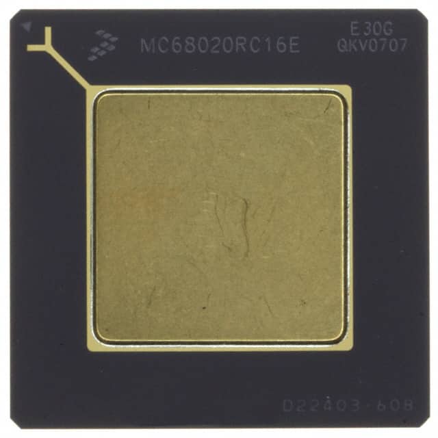
- Part No.:
- MC68020RC16E
- Manufacturer:
- NXP Semiconductors
- Category:
- Microprocessors
- Package:
- 114-BPGA
- Datasheet:
-
 MC68020RC16E.pdf
- Description:
- IC MPU M680X0 16MHZ 114PGA
- Quantity:
- Payment:

- Shipping:

Inventory:1,856
Please send an inquiry. Send us your inquiry, and we will respond immediately.
Product details
Overview
MC68020RC16E from Motorola (later Freescale) is a 32-bit, second-generation enhanced microprocessor with full 32-bit data and address buses (A31–A0, D31–D0), on-chip 256-byte instruction cache, and support for coprocessor interface (CP0–CP3). It operates at 16 MHz, uses a pipelined architecture with five-stage instruction execution, and targets embedded control and workstation-class systems requiring virtual memory and supervisor/user privilege separation.
For engineers reviewing the MC68020RC16E datasheet, MC68020RC16E pinout, MC68020RC16E application, or MC68020RC16E equivalent, key selection criteria include its 16 MHz clock rating, 32-bit synchronous/asynchronous bus interface, coprocessor handshake protocol (AS, DSACK0/DSACK1), exception vector table layout, and compatibility with M68000-family toolchains and operating systems like VxWorks and early AmigaOS variants.
Technical Context
The MC68020RC16E implements a five-stage pipeline (fetch, decode, execute, address generation, write-back) and supports dynamic bus sizing via SIZ1/SIZ0 signals for 8-, 16-, or 32-bit transfers. Its on-chip 256-byte instruction cache reduces average instruction fetch latency and enables prefetching of up to four instructions.
It features a full 32-bit external bus with asynchronous timing controlled by AS, DTACK, and DSACK0/DSACK1, supports bus arbitration via BR/BG/BGACK, and provides dedicated coprocessor interface signals (CPA, CPB, CPC, CPD) for concurrent operation with FPUs or MMUs. Exception handling includes 256-vector table addressing and supervisor/user mode stack frame management.
Key Specifications
| Parameter | Value and Actual Design Meaning |
|---|---|
| Clock Frequency | 16 MHz maximum - defines instruction throughput ceiling and synchronizes all internal pipeline stages and external bus timing. |
| Data Bus Width | 32-bit (D31–D0) - enables single-cycle transfer of full 32-bit operands and addresses, eliminating byte/word alignment penalties in native code. |
| Address Bus Width | 32-bit (A31–A0) - supports 4 GB linear address space, required for flat memory models and virtual memory implementations. |
| Instruction Cache | 256-byte on-chip - improves average instruction fetch latency by reducing external memory accesses; not configurable or writable. |
| Bus Interface Type | Asynchronous with DSACK0/DSACK1 handshaking - allows interfacing with diverse memory and peripheral speeds without fixed wait-state constraints. |
| Privilege Modes | Supervisor and User - enforces hardware-level memory protection and OS kernel isolation via status register (SR) bit 13. |
| Coprocessor Support | Dedicated CP0–CP3 interface with CPA/CPC/CPD handshake - enables concurrent FPU or MMU operation without CPU stall cycles. |
Pinout & Package
MC68020RC16E is housed in a 132-pin ceramic PGA (Pin Grid Array) package with 0.1-inch pin spacing, designed for high-reliability industrial and military applications. Thermal and mechanical data confirm a 1.27 mm pin diameter and 2.54 mm pitch.
| Pin/Terminal | Circuit Role | Design Meaning |
|---|---|---|
| CLK | Clock Input | Accepts TTL-compatible 16 MHz square wave; drives internal pipeline and bus timing generator. |
| AS | Address Strobe | Active-low signal indicating valid address on A31–A0; initiates bus cycle timing sequence. |
| DTACK | Data Transfer Acknowledge | Active-low input confirming external device readiness; determines number of wait states in read/write cycles. |
| DSACK0/DSACK1 | Data Strobe Acknowledge Pair | Two-wire handshake specifying data size (byte/word/long) and completion of synchronous transfers. |
| BR/BG/BGACK | Bus Request/Grant/Grant Acknowledge | Three-wire arbitration protocol enabling DMA controllers or other masters to seize bus control. |
| FC2–FC0 | Function Code Outputs | Encode current bus cycle type (data space, program space, I/O space, supervisor/user mode) for memory mapping logic. |
| CPA–CPD | Coprocessor Interface Signals | Control lines coordinating instruction execution, operand transfer, and exception signaling between CPU and coprocessor. |
Key Features
| Feature | Design Value |
|---|---|
| Five-stage pipelined execution | Enables overlapping instruction fetch, decode, and execution - achieves ~1.5 MIPS at 16 MHz with reduced average CPI. |
| 256-byte on-chip instruction cache | Reduces external memory bandwidth demand and instruction fetch latency - critical for deterministic real-time response in control loops. |
| Full 32-bit address and data buses | Eliminates software address masking and data packing overhead - simplifies C compiler code generation and OS memory management. |
| Hardware-supported virtual memory | Provides MMU-ready interface (including function codes and bus error vectors) - enables implementation of paged memory systems without external translation logic. |
| Dedicated coprocessor interface (CP0–CP3) | Allows concurrent FPU or MMU operation with zero-cycle context switching - avoids pipeline stalls during floating-point or address translation operations. |
Applications
| Industrial CNC Controllers | Legacy Workstation Terminals |
|---|---|
|
Use Scenario: Real-time motion control in multi-axis machine tools requiring deterministic interrupt response and precise timer synchronization. IC Role / Device Role / Timing Role: Main CPU executing G-code interpreter and servo loop scheduler; manages dual-ported RAM for position buffer exchange. Use Value: 32-bit address space enables direct access to large encoder buffers; pipelined execution ensures sub-100 µs worst-case interrupt latency. |
Use Scenario: High-performance terminal emulation and local graphics rendering in X Window System-based workstations (e.g., Sun-3 compatible). IC Role / Device Role / Timing Role: Host processor driving custom video controller and SCSI host adapter; executes Unix-like OS kernel and window manager. Use Value: On-chip instruction cache reduces display list fetch latency; coprocessor interface supports optional 68881 FPU for geometry calculations. |
| Avionics Data Acquisition Units | Early Digital Signal Analyzers |
|
Use Scenario: Ruggedized flight data recorders capturing sensor streams (pressure, temperature, acceleration) under MIL-STD-810 environmental conditions. IC Role / Device Role / Timing Role: Central controller managing ADC sampling, EEPROM logging, and ARINC-429 serial interface. Use Value: Ceramic PGA package ensures thermal stability across −55°C to +125°C; bus arbitration allows concurrent DMA transfers to flash storage. |
Use Scenario: Benchtop instruments performing FFT-based spectral analysis on analog input signals sampled at 10+ MS/s. IC Role / Device Role / Timing Role: Control processor coordinating high-speed ADC, SRAM buffer management, and GPIB/IEEE-488 output interface. Use Value: 32-bit data bus enables single-cycle transfer of complex FFT coefficients; instruction cache improves loop execution in real-time filtering routines. |
Equivalent & Alternatives
The following parts are listed as comparable options for similar 32-bit microprocessor applications.
| Alternative Part | Technical Difference | Application Difference | Selection Advice |
|---|---|---|---|
| MC68020RC20E | 20 MHz clock rating; identical pinout, cache, and bus architecture; higher power consumption (typ. 1.8 W vs. 1.5 W). | Supports higher instruction throughput in compute-bound tasks but requires tighter thermal design and faster memory timing. | Select when system clock budget allows 20 MHz and memory subsystem can meet shorter access time requirements. |
| MC68EC020RC16B | Same 16 MHz speed but 24-bit address bus (A23–A0); no VMEbus support; lacks some coprocessor handshake signals. | Targeted at cost-sensitive embedded systems with ≤16 MB memory; unsuitable for full 4 GB virtual memory or VMEbus expansion. | Select only for memory-constrained designs where full 32-bit addressing is unnecessary and BGA packaging is preferred. |
Compared with MC68020RC16E, the RC20E offers higher performance at the cost of thermal headroom, while the MC68EC020RC16B trades address space and bus flexibility for lower cost and power - making MC68020RC16E the balanced choice for full-featured 32-bit embedded control.
Availability
MC68020RC16E is available at Aetrix Electronics and suitable for industrial CNC controllers, avionics data acquisition units, and legacy workstation terminals requiring stable component supply and long-term obsolescence management.
Supply support for MC68020RC16E includes scheduled delivery planning, volume procurement assistance, BOM continuity management, traceable sourcing, and lifecycle availability coordination for OEM customers, industrial embedded developers, connected-device designers, and electronics production programs.
Manufacturer
Motorola Semiconductor (later Freescale Semiconductor) was a pioneering U.S. semiconductor manufacturer known for the 68000 family, RF power transistors, and automotive ICs before its acquisition by NXP in 2015.
The MC68020RC16E belongs to the M68000 microprocessor family, designed for high-reliability embedded computing and workstation platforms requiring full 32-bit processing, virtual memory support, and coprocessor extensibility.
FAQ
What is the maximum operating frequency of the MC68020RC16E?
The MC68020RC16E is rated for a maximum clock frequency of 16 MHz, as specified in Section 10.3 (AC Electrical Characteristics) of the M68020 User's Manual. This frequency defines the upper limit for reliable pipeline operation, bus timing, and instruction execution - exceeding it risks timing violations, data corruption, or undefined behavior. The '16' in the suffix explicitly denotes this speed grade.
Does the MC68020RC16E include an integrated memory management unit (MMU)?
No, the MC68020RC16E does not integrate an MMU. It provides hardware support for virtual memory through dedicated bus signals (FC2–FC0), exception vectors, and status register bits, but requires an external MMU such as the MC68851 to implement paged memory translation. This modular design allows system architects to select MMU features and performance independently of the CPU.
What package type is used for the MC68020RC16E?
The MC68020RC16E uses a 132-pin ceramic Pin Grid Array (PGA) package, as confirmed in Section 11.2.1 (Pin Assignments and Package Dimensions) of the M68020 User's Manual. This package features a 0.1-inch pin pitch, gold-plated pins, and is qualified for extended temperature ranges - making it suitable for aerospace, industrial, and military applications where reliability under thermal stress is critical.
Can the MC68020RC16E interface directly with a 68881 floating-point unit?
Yes, the MC68020RC16E supports direct interface with the MC68881 FPU via its dedicated coprocessor interface (CP0–CP3 signals). The CPU automatically handles operand transfer, exception synchronization, and instruction dispatch without software intervention - enabling concurrent integer and floating-point execution as documented in Section 7 of the M68020 User's Manual.
What is the purpose of the DSACK0 and DSACK1 signals on the MC68020RC16E?
The DSACK0 and DSACK1 signals on the MC68020RC16E form a two-wire handshake that indicates data transfer completion and specifies the effective data size (byte, word, or long word) during synchronous bus cycles. Unlike DTACK, which controls asynchronous timing, DSACK0/DSACK1 enable precise coordination with synchronous peripherals and memory devices - essential for high-speed burst transfers and coprocessor communication.
MC68020RC16E Specifications
- Product attributes
- Attribute value
- Manufacturer:
- NXP Semiconductors
- Package/Case:
- 114-BPGA
- Series:
- M680x0
- Packaging:
- Tray
- Product Status:
- Obsolete
- Core Processor:
- 68020
- Number of Cores/Bus Width:
- 1 Core, 32-Bit
- Speed:
- 16MHz
- Co-Processors/DSP:
- -
- RAM Controllers:
- -
- Graphics Acceleration:
- No
- Display & Interface Controllers:
- -
- Ethernet:
- -
- SATA:
- -
- USB:
- -
- Voltage - I/O:
- 5.0V
- Operating Temperature:
- 0°C ~ 70°C (TA)
- Grade:
- -
- Qualification:
- -
- Security Features:
- -
- Mounting Type:
- Through Hole
- Supplier Device Package:
- 114-PGA (34.55x34.55)
- Additional Interfaces:
- -
MC68020RC16E FAQ
1.How can I place an order for MC68020RC16E through Aetrix?
Please submit a Request for Quotation (RFQ) for MC68020RC16E on Aetrix. Our sales agent will provide a competitive quotation and guide you through the order confirmation once you accept the terms.
2.Are the price and stock information for MC68020RC16E reliable?
The price and inventory of MC68020RC16E are updated periodically and may fluctuate due to market conditions. Stock and pricing data are typically refreshed every 24 hours. Quotation validity for MC68020RC16E is usually 5 days.
3.What payment methods are accepted for MC68020RC16E?
We accept Wire Transfer, PayPal, Credit Card, Western Union, MoneyGram, and Escrow for MC68020RC16E transactions.
Note: Certain payment methods may incur a processing fee.
4.How is shipping managed for MC68020RC16E?
MC68020RC16E orders can be shipped via leading logistics carriers, including DHL, UPS, FedEx, TNT, or Registered Mail.
Once your MC68020RC16E order is processed, you will receive an email with the shipment details and tracking number.
Note: Tracking information may take up to 24 hours to appear. Express delivery typically takes 3–5 business days.
5.How can I obtain technical support or documentation for MC68020RC16E?
For technical support, including MC68020RC16E datasheets, pinout diagrams, or application guidance, please contact our engineering support team. They can provide detailed documentation and assistance for your MC68020RC16E requirements.
6.How does Aetrix verify that MC68020RC16E is sourced from the original manufacturer or authorized distributors?
All MC68020RC16E products on Aetrix are procured from qualified distributors and authorized channels. Our dedicated quality assurance team conducts strict verification, including traceability checks and, if necessary, third-party testing. This ensures that MC68020RC16E meets industry standards.
7.What is the process for return or replacement of MC68020RC16E?
All MC68020RC16E units undergo pre-shipment inspection (PSI). If there is an issue with MC68020RC16E, returns or replacements are accepted under the following conditions:
1.Quantity discrepancies, incorrect items, or visible external defects (such as breakage or corrosion), acknowledged by Aetrix.
2.The issue is reported within 90 days of delivery.
3.The MC68020RC16E part is unused and in its original packaging.
Return procedure for MC68020RC16E:
1.Submit a request within 90 days.
2.Obtain a Return Material Authorization (RMA) from Aetrix.
MC68020RC16E Tags

-
AT91SAM9260B-CU-999
Microchip Technology
-
AT91SAM9G25-CU
Microchip Technology

-
ATSAMA5D27C-CU
Microchip Technology
-
AT91SAM9X35-CU
Microchip Technology
-
AT91SAM9X25-CU
Microchip Technology

-
MCIMX6Y2CVM08AB
NXP Semiconductors
.JPG)
-
AM3352BZCZ100
Texas Instruments
-
AT91SAM9260B-CU
Microchip Technology

-
AT91SAM9260B-QU
Microchip Technology

-
ATSAMA5D31A-CU
Microchip Technology
-
AT91SAM9G20B-CU-999
Microchip Technology
-
MCIMX6Y2CVM05AB
NXP Semiconductors
Tech Hub

A practical engineering guide to 3.3V and 5V logic compatibility, input thresholds, resistor dividers, translator ICs, MOSFET level shifting, I2C pull-ups, timing limits and power-sequencing risks.

The 74HC595 uses push-pull logic outputs, while the TPIC6B595 uses 50 V open-drain DMOS sinks for higher-power loads. This guide compares timing, current limits, 3.3 V interfacing, load wiring, thermal…

The 74HC595 converts serial data into eight stable parallel outputs. This guide covers pin functions, shift and storage timing, OE and MR behavior, drive-current limits, cascading, voltage compatibilit…

A technical comparison of level-sensitive latches and edge-triggered flip-flops, covering timing windows, setup and hold limits, master–slave operation, time borrowing, race-through, HDL inference and…

A D latch stores one bit while Enable controls when data can pass. This reference covers gate-level operation, truth tables, transparency, setup and hold timing, LE versus OE, common ICs and practical …

An SR latch stores one bit through cross-coupled feedback. This engineering reference covers NOR and NAND implementations, truth tables, forbidden-state recovery, gated operation, switch debouncing, fa…

Latch circuits retain one bit through feedback. This technical reference covers SR and D latches, truth tables, transparency, timing limits, latch-versus-flip-flop behavior, applications and common log…

An engineering guide to LED driver operation, constant-current and constant-voltage outputs, linear and switching topologies, dimming, IC selection, calculations, replacement compatibility, and fault c…

Operational amplifier guide covering op amp basics, feedback, ideal vs real op amps, common configurations, buffer circuits, offset, bias current, gain-bandwidth, slew rate, rail-to-rail limits and sel…

Jumper cables guide covering safe connection order, red and black clamp placement, final ground connection, cable gauge, length, clamp quality, copper vs CCA cables, jump starter comparison and battery…


