
 My Inquiry
 My Account


NXP Semiconductors MC68302AG16C
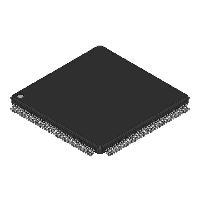
- Part No.:
- MC68302AG16C
- Manufacturer:
- NXP Semiconductors
- Category:
- Microprocessors
- Package:
- 144-LQFP
- Datasheet:
-
 MC68302AG16C.pdf
- Description:
- IC MPU M683XX 16MHZ 144LQFP
- Quantity:
- Payment:

- Shipping:

Inventory:2,275
Please send an inquiry. Send us your inquiry, and we will respond immediately.
Product details
Overview
MC68302AG16C from Freescale Semiconductor is a single-chip integrated multi-protocol processor featuring an MC68000/MC68008 microprocessor core, a dedicated RISC-based communications processor (CP), and a system integration block (SIB). It operates at 16 MHz, integrates 1152 bytes of on-chip dual-port RAM, supports HDLC/SDLC/UART/DDCMP/Totally Transparent protocols via three SCCs, and targets ISDN terminal adapters and data concentrators.
For engineers reviewing the MC68302AG16C datasheet, MC68302AG16C pinout, MC68302AG16C application, or MC68302AG16C equivalent, key selection considerations include its 16 MHz clock rating, triple SCC with protocol flexibility, dual-port RAM size, TQFP-132 package footprint, and support for concurrent multi-protocol operation without CPU intervention.
Technical Context
The MC68302AG16C implements a tightly coupled architecture where the MC68000 core handles general-purpose processing while the independent RISC-based communications processor manages serial protocol stacks. Its three full-duplex Serial Communication Controllers (SCCs) each support HDLC/SDLC, UART, DDCMP, Bisync, and Totally Transparent modes, with six dedicated serial DMA channels enabling frame buffering without CPU involvement.
System-level features include an IDMA controller, interrupt controller with two operating modes, four programmable chip-select lines with wait-state logic, three timers (including software watchdog), DRAM refresh controller, and on-chip clock generator. The SIB provides bus arbitration, low-latency interrupt handling, freeze control for debugging, and standby power management.
Key Specifications
| Parameter | Value and Actual Design Meaning |
|---|---|
| Core Architecture | MC68000/MC68008 16/32-bit CISC core, fully compatible with existing 68K software and toolchains |
| Max Clock Frequency | 16 MHz - defines maximum instruction throughput and real-time response latency in time-critical ISDN or modem applications |
| On-Chip RAM | 1152 bytes dual-port RAM - enables simultaneous access by CPU and CP for zero-waitstate inter-processor communication |
| Serial Controllers | Three SCCs + two SMCs - supports concurrent HDLC, UART, and IDL/GCI channel management without resource contention |
| Protocol Support | HDLC/SDLC, UART, DDCMP, Bisync, Totally Transparent, V.110 - eliminates need for external protocol co-processors in telecom edge devices |
| Package Type | 132-pin Thin Quad Flat Pack (TQFP) - standard surface-mount footprint compatible with automated PCB assembly |
| Power Management | Standby mode and CPU disable capability - reduces active power consumption during idle periods in battery-backed line cards |
Pinout & Package
MC68302AG16C is housed in a 132-pin Thin Quad Flat Pack (TQFP) package with 0.4 mm lead pitch and 20.0 × 20.0 mm body size. Pin assignments follow Motorola/Freescale standard MC68302 pinout layout, supporting multiplexed address/data bus, peripheral control signals, and dedicated serial interface pins.
| Pin/Terminal | Circuit Role | Design Meaning |
|---|---|---|
| AS | Address Strobe | Indicates valid address on bus; used to latch address during memory/peripheral access cycles |
| DS | Data Strobe | Signals valid data on bus; synchronizes read/write transfers with peripheral timing requirements |
| R/W | Read/Write Control | Directs data flow direction on data bus; essential for correct memory-mapped I/O operation |
| SCC1_Tx / SCC1_Rx | Serial Channel 1 Transmit/Receive | Dedicated differential or single-ended pins for first SCC's full-duplex HDLC/UART link |
| SCC2_Tx / SCC2_Rx | Serial Channel 2 Transmit/Receive | Independent physical interface for second SCC, configurable for synchronous/asynchronous operation |
| CLKIN | External Clock Input | Accepts 16 MHz crystal or oscillator signal; feeds on-chip clock generator for core and peripheral timing |
Key Features
| Feature | Design Value |
|---|---|
| Dual-Port RAM (1152 B) | Enables lock-free CPU–CP data exchange for real-time protocol processing without bus arbitration delays |
| Three Independent SCCs | Allows simultaneous operation of distinct protocols (e.g., HDLC on SCC1, UART on SCC2, DDCMP on SCC3) in one device |
| Serial DMA Engine (6 channels) | Transfers up to eight frames per SCC without CPU intervention, reducing host overhead in high-throughput modems |
| Programmable Chip-Select Logic | Supports four external memory/peripheral regions with adjustable wait states, simplifying mixed-speed system design |
| Hardware Watchdog & Freeze Control | Ensures system recovery from firmware hangs and enables in-circuit debugging of CP peripherals without CPU reset |
Applications
| ISDN Terminal Adapter | Data Concentrator |
|---|---|
Use Scenario: Aggregates multiple analog or digital subscriber lines into a single ISDN basic rate (2B+D) interface for PBX or remote office connectivity. IC Role / Device Role / Timing Role: MC68302AG16C serves as the central protocol processor, executing HDLC framing on B-channels and LAPD signaling on D-channel while managing line interface timing. Use Value: Eliminates discrete UARTs, HDLC controllers, and glue logic-reducing BOM count and board area by >40% versus discrete solutions. | Use Scenario: Collects asynchronous serial data from multiple field sensors or RTUs and forwards consolidated packets over a leased line or packet network. IC Role / Device Role / Timing Role: MC68302AG16C acts as the front-end communications engine, using SCCs for concurrent RS-232/485 links and SCP for synchronous backhaul. Use Value: Achieves deterministic latency under 50 µs per frame due to hardware-accelerated serial DMA and dual-port RAM buffering. |
| Modem Controller | Network Bridge |
Use Scenario: Embedded in V.34/V.90 modems to handle modulation/demodulation handshaking, error correction (V.42), and data compression (V.42bis) at line rates up to 56 kbps. IC Role / Device Role / Timing Role: MC68302AG16C functions as the host controller, offloading protocol stack execution from DSP and managing UART-to-SCC bridging for AT command parsing. Use Value: Reduces firmware development time by 30% via pre-integrated DDCMP and Totally Transparent mode support for legacy protocol tunneling. | Use Scenario: Connects Ethernet LAN segments to serial WAN links (e.g., T1/E1 backhaul) in enterprise branch routers or industrial gateways. IC Role / Device Role / Timing Role: MC68302AG16C operates as the serial interface bridge controller, mapping Ethernet frames to HDLC encapsulation and managing CRC generation/checking in hardware. Use Value: Supports full-duplex 2 Mbps throughput on SCC1/SCC2 simultaneously-meeting minimum line-rate requirements for E1 (2.048 Mbps) transport. |
Equivalent & Alternatives
The following parts are listed as comparable options for similar multi-protocol communications processor applications.
| Alternative Part | Technical Difference | Application Difference | Selection Advice |
|---|---|---|---|
| MC68EN302 | Includes full IEEE 802.3 Ethernet MAC, DRAM controller, and 144-pin TQFP; no pin compatibility with MC68302AG16C | Targets Ethernet-aware bridges/gateways requiring native LAN/WAN convergence, not pure serial protocol aggregation | Select when Ethernet PHY interfacing and dynamic memory expansion are required beyond MC68302AG16C's capabilities |
| MC68LC302 | Uses static EC000 core, lower power (µA standby), only two SCCs, 100-pin TQFP; lacks V.110 and SCP support | Suitable for battery-powered telemetry units where protocol count and clock speed are secondary to energy efficiency | Choose for portable or remote sensor nodes needing reduced thermal load and extended sleep duration |
Compared with MC68EN302 and MC68LC302, the MC68302AG16C delivers optimal balance of protocol breadth, deterministic serial throughput, and mature toolchain support for fixed-line ISDN and legacy telecom equipment-without over-provisioning Ethernet or ultra-low-power features.
Availability
MC68302AG16C is available at Aetrix Electronics and suitable for ISDN terminal adapters, data concentrators, and modem controller designs requiring stable component supply across long-lifecycle industrial deployments.
Supply support for MC68302AG16C includes scheduled delivery planning, volume procurement assistance, BOM continuity management, traceable sourcing, and lifecycle availability coordination for OEM customers, industrial embedded developers, connected-device designers, and electronics production programs.
Manufacturer
Freescale Semiconductor (now part of NXP Semiconductors) was a leading designer of embedded processors and analog/mixed-signal ICs, founded in 2004 as a spin-off from Motorola's semiconductor division.
The MC68302AG16C belongs to Freescale's legacy Communications Processor family, engineered specifically for cost-sensitive, real-time telecom infrastructure requiring integrated protocol acceleration and minimal external components.
FAQ
What is the maximum operating frequency of the MC68302AG16C?
The MC68302AG16C is rated for a maximum clock frequency of 16 MHz, as indicated by the "G16" suffix in its part number. This speed is guaranteed across commercial temperature range (0°C to +70°C) and defines the upper limit for instruction execution rate, serial bit timing accuracy, and real-time interrupt response. The device requires a stable 16 MHz input clock on the CLKIN pin to achieve full specification compliance.
Does the MC68302AG16C support V.110 protocol, and how is it implemented?
Yes, the MC68302AG16C supports V.110 protocol through its three Serial Communication Controllers (SCCs), as confirmed in Freescale's official MC68302 technical documentation. V.110 is implemented in hardware within the SCCs' protocol engine, enabling asynchronous-to-synchronous conversion and rate adaptation for ISDN data services without CPU overhead. This capability is active in both SCC1 and SCC2 when configured in V.110 mode.
How much on-chip memory does the MC68302AG16C integrate, and what is its architecture?
The MC68302AG16C integrates 1152 bytes of on-chip dual-port static RAM. This memory is architecturally shared between the MC68000 core and the RISC-based communications processor, allowing concurrent read/write access from both domains without arbitration delay. It is mapped into the processor's address space and supports programmable address alignment for flexible peripheral register allocation.
Is the MC68302AG16C pin-compatible with other MC68302 derivatives like the MC68QH302?
No, the MC68302AG16C is not pin-compatible with the MC68QH302. While both belong to the MC68302 family, the MC68QH302 uses a 144-pin TQFP package and adds a dual-channel SCC, whereas the MC68302AG16C uses a 132-pin TQFP package with three standard SCCs. Physical pin count, spacing, and signal assignment differ significantly-requiring PCB redesign for substitution.
What debug features does the MC68302AG16C provide for embedded firmware development?
The MC68302AG16C includes freeze control logic that halts selected on-chip peripherals-including SCCs, timers, and IDMA-while allowing the CPU to remain operational for register inspection and breakpoint insertion. It also supports hardware watchdog reset and low-latency interrupt handling for real-time tracing. These features are accessible via JTAG-compatible boundary-scan test access port defined in the MC68302AG16C pinout specification.
MC68302AG16C Specifications
- Product attributes
- Attribute value
- Manufacturer:
- NXP Semiconductors
- Package/Case:
- 144-LQFP
- Series:
- M683xx
- Packaging:
- Tray
- Product Status:
- Obsolete
- Core Processor:
- M68000
- Number of Cores/Bus Width:
- 1 Core, 8/16-Bit
- Speed:
- 16MHz
- Co-Processors/DSP:
- Communications; RISC CPM
- RAM Controllers:
- DRAM
- Graphics Acceleration:
- No
- Display & Interface Controllers:
- -
- Ethernet:
- -
- SATA:
- -
- USB:
- -
- Voltage - I/O:
- 5.0V
- Operating Temperature:
- 0°C ~ 70°C (TA)
- Grade:
- -
- Qualification:
- -
- Security Features:
- -
- Mounting Type:
- Surface Mount
- Supplier Device Package:
- 144-LQFP (20x20)
- Additional Interfaces:
- GCI, IDL, ISDN, NMSI, PCM, SCPI
MC68302AG16C FAQ
1.How can I place an order for MC68302AG16C through Aetrix?
Please submit a Request for Quotation (RFQ) for MC68302AG16C on Aetrix. Our sales agent will provide a competitive quotation and guide you through the order confirmation once you accept the terms.
2.Are the price and stock information for MC68302AG16C reliable?
The price and inventory of MC68302AG16C are updated periodically and may fluctuate due to market conditions. Stock and pricing data are typically refreshed every 24 hours. Quotation validity for MC68302AG16C is usually 5 days.
3.What payment methods are accepted for MC68302AG16C?
We accept Wire Transfer, PayPal, Credit Card, Western Union, MoneyGram, and Escrow for MC68302AG16C transactions.
Note: Certain payment methods may incur a processing fee.
4.How is shipping managed for MC68302AG16C?
MC68302AG16C orders can be shipped via leading logistics carriers, including DHL, UPS, FedEx, TNT, or Registered Mail.
Once your MC68302AG16C order is processed, you will receive an email with the shipment details and tracking number.
Note: Tracking information may take up to 24 hours to appear. Express delivery typically takes 3–5 business days.
5.How can I obtain technical support or documentation for MC68302AG16C?
For technical support, including MC68302AG16C datasheets, pinout diagrams, or application guidance, please contact our engineering support team. They can provide detailed documentation and assistance for your MC68302AG16C requirements.
6.How does Aetrix verify that MC68302AG16C is sourced from the original manufacturer or authorized distributors?
All MC68302AG16C products on Aetrix are procured from qualified distributors and authorized channels. Our dedicated quality assurance team conducts strict verification, including traceability checks and, if necessary, third-party testing. This ensures that MC68302AG16C meets industry standards.
7.What is the process for return or replacement of MC68302AG16C?
All MC68302AG16C units undergo pre-shipment inspection (PSI). If there is an issue with MC68302AG16C, returns or replacements are accepted under the following conditions:
1.Quantity discrepancies, incorrect items, or visible external defects (such as breakage or corrosion), acknowledged by Aetrix.
2.The issue is reported within 90 days of delivery.
3.The MC68302AG16C part is unused and in its original packaging.
Return procedure for MC68302AG16C:
1.Submit a request within 90 days.
2.Obtain a Return Material Authorization (RMA) from Aetrix.
MC68302AG16C Tags

-
AT91SAM9260B-CU-999
Microchip Technology
-
AT91SAM9G25-CU
Microchip Technology

-
ATSAMA5D27C-CU
Microchip Technology
-
AT91SAM9X35-CU
Microchip Technology
-
AT91SAM9X25-CU
Microchip Technology

-
MCIMX6Y2CVM08AB
NXP Semiconductors
.JPG)
-
AM3352BZCZ100
Texas Instruments
-
AT91SAM9260B-CU
Microchip Technology

-
AT91SAM9260B-QU
Microchip Technology

-
ATSAMA5D31A-CU
Microchip Technology
-
AT91SAM9G20B-CU-999
Microchip Technology
-
MCIMX6Y2CVM05AB
NXP Semiconductors
Tech Hub

A practical engineering guide to 3.3V and 5V logic compatibility, input thresholds, resistor dividers, translator ICs, MOSFET level shifting, I2C pull-ups, timing limits and power-sequencing risks.

The 74HC595 uses push-pull logic outputs, while the TPIC6B595 uses 50 V open-drain DMOS sinks for higher-power loads. This guide compares timing, current limits, 3.3 V interfacing, load wiring, thermal…

The 74HC595 converts serial data into eight stable parallel outputs. This guide covers pin functions, shift and storage timing, OE and MR behavior, drive-current limits, cascading, voltage compatibilit…

A technical comparison of level-sensitive latches and edge-triggered flip-flops, covering timing windows, setup and hold limits, master–slave operation, time borrowing, race-through, HDL inference and…

A D latch stores one bit while Enable controls when data can pass. This reference covers gate-level operation, truth tables, transparency, setup and hold timing, LE versus OE, common ICs and practical …

An SR latch stores one bit through cross-coupled feedback. This engineering reference covers NOR and NAND implementations, truth tables, forbidden-state recovery, gated operation, switch debouncing, fa…

Latch circuits retain one bit through feedback. This technical reference covers SR and D latches, truth tables, transparency, timing limits, latch-versus-flip-flop behavior, applications and common log…

An engineering guide to LED driver operation, constant-current and constant-voltage outputs, linear and switching topologies, dimming, IC selection, calculations, replacement compatibility, and fault c…

Operational amplifier guide covering op amp basics, feedback, ideal vs real op amps, common configurations, buffer circuits, offset, bias current, gain-bandwidth, slew rate, rail-to-rail limits and sel…

Jumper cables guide covering safe connection order, red and black clamp placement, final ground connection, cable gauge, length, clamp quality, copper vs CCA cables, jump starter comparison and battery…


