
 My Inquiry
 My Account


NXP Semiconductors MC68306CEH16B
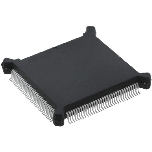
- Part No.:
- MC68306CEH16B
- Manufacturer:
- NXP Semiconductors
- Category:
- Microprocessors
- Package:
- 132-BQFP Bumpered
- Datasheet:
-
 MC68306CEH16B.pdf
- Description:
- IC MPU M683XX 16MHZ 132PQFP
- Quantity:
- Payment:

- Shipping:

Inventory:1,752
Please send an inquiry. Send us your inquiry, and we will respond immediately.
Product details
Overview
MC68306CEH16B from Motorola is an integrated 68EC000-based microcontroller unit featuring a 16.67-MHz EC000 core, two-channel DUART (identical to MC68681), DRAM controller supporting up to 64 Mbytes, eight programmable chip selects, and IEEE 1149.1 JTAG test interface - deployed in industrial embedded control systems requiring compact, code-compatible 68000-class processing with serial I/O and dynamic memory management.
For engineers reviewing the MC68306CEH16B datasheet, MC68306CEH16B pinout, MC68306CEH16B application, or MC68306CEH16B equivalent, key selection considerations include 128-pin QFP package compatibility, 5-V operation, 24-bit address/16-bit data bus width, DRAM refresh timing configuration, and interrupt vectoring support for real-time OS integration.
Technical Context
The MC68306CEH16B integrates an EC000 CPU core delivering 2.4 MIPS at 16.67 MHz with full MC68000 instruction set compatibility and supervisor/user mode protection. Its on-chip peripherals include a dual-channel UART with independent baud rate generators (up to 38.4 kbps), 16-bit timer/counter, and DRAM controller supporting CAS-before-RAS refresh for 4M×1 and 16M×1 DRAMs.
System-level glue logic is embedded via eight programmable chip selects (each configurable for 1-Mbyte or 16-Mbyte spaces within 4-Gbyte address range), a seven-level priority interrupt controller with maskable IRQ inputs, and a bus watchdog timer programmable up to 4096 clock cycles - all synchronized to the internal 16.67-MHz clock domain.
Key Specifications
| Parameter | Value and Actual Design Meaning |
|---|---|
| Core Architecture | 68EC000 32-bit CPU, fully code-compatible with MC68000 and MC68EC000 |
| Operating Frequency | 16.67 MHz - enables 2.4 MIPS performance with zero-wait-state DRAM access using 80-ns parts |
| Memory Interface | 24-bit address bus / 16-bit data bus - supports 4-Gbyte linear addressing space |
| DRAM Support | Up to 64 Mbytes using 16M×1 DRAMs with programmable CAS-before-RAS refresh timer |
| Serial Interface | Dual-channel UART (MC68681-equivalent) with 4-byte RX / 2-byte TX FIFOs and full modem control (RTS/CTS per channel) |
| Package Type | 128-pin plastic quad flat pack (QFP), 0.8-mm lead pitch - surface-mount footprint optimized for industrial PCB density |
| Supply Voltage | 5.0 V ±5% - compatible with legacy 5-V system rails and TTL-level peripheral interfacing |
Pinout & Package
MC68306CEH16B is housed in a 128-pin gull-wing plastic quad flat pack (QFP) with 0.8-mm lead spacing. The package provides dedicated power/ground distribution (20 pins) to minimize ground bounce across functional blocks including CPU core, DRAM controller, and serial I/O.
| Pin/Terminal | Circuit Role | Design Meaning |
|---|---|---|
| PA0–PA7 | Port A Data Lines | 8-bit bidirectional parallel I/O port, individually configurable as input or output via internal registers |
| PB0–PB7 | Port B Data Lines | 8-bit bidirectional port multiplexed with IRQ/IP and IACK lines - function selected by internal mode register |
| A19–A16, A15/DRAMA14–A1/DRAMA0 | Address/DRAM Address Lines | Upper address bits and DRAM row/column multiplexed address lines - decoupled from chip select logic to enable flexible memory mapping |
| CS0–CS7 | Chip Select Outputs | Eight programmable outputs defining up to eight 1-Mbyte or four 16-Mbyte memory/peripheral spaces anywhere in 4-Gbyte address space |
| RxDA/RxDB, TxDA/TxDB | UART Channel A/B Serial I/O | Full-duplex asynchronous/synchronous receive/transmit lines - each channel supports independent baud rate, parity, and stop-bit configuration |
| TCK/TMS/TDI/TDO/TRST | JTAG Boundary Scan Interface | IEEE 1149.1-compliant test access port enabling board-level interconnect verification and in-system debugging |
Key Features
| Feature | Design Value |
|---|---|
| Integrated DUART | Eliminates need for external MC68681, reducing BOM count and PCB area while preserving identical register-level software compatibility |
| Programmable DRAM Controller | Enables direct connection to industry-standard 4M×1 or 16M×1 DRAMs without external refresh logic or address multiplexing circuitry |
| Eight Chip Selects | Replaces discrete address decoders and wait-state generators - each CS independently configurable for base address, size, and timing |
| Bus Watchdog Timer | Prevents system lockup by terminating stalled bus cycles after programmable timeout (up to 4096 clocks), improving field reliability |
| JTAG Test Access | Supports boundary scan testing of solder joints and interconnects without physical probe access - critical for high-density industrial assemblies |
Applications
| Industrial PLC Controller | Telecom Line Card |
|---|---|
Use Scenario: Real-time logic execution and I/O scanning in programmable logic controllers with serial HMI and remote diagnostics. IC Role / Device Role / Timing Role: Central processing and peripheral integration unit - executes ladder logic, manages RS-232/485 communications, and controls DRAM-based program storage. Use Value: Reduces component count by integrating CPU, UART, DRAM controller, and interrupt management - enabling compact, fanless enclosure designs with deterministic response under 10-ms scan cycles. | Use Scenario: Protocol bridging and status monitoring in carrier-grade line interface cards handling T1/E1 framing and alarm reporting. IC Role / Device Role / Timing Role: Embedded controller managing serial telemetry channels, DRAM-based buffer memory, and interrupt-driven event logging. Use Value: Dual UART channels support simultaneous local maintenance port and remote network management interface - eliminating need for separate communication ICs and simplifying firmware update paths. |
| Medical Diagnostic Equipment | Avionics Data Acquisition Unit |
Use Scenario: Sensor data aggregation and display control in portable ultrasound or ECG devices requiring deterministic I/O and low-power operation. IC Role / Device Role / Timing Role: System-on-chip processor handling analog-to-digital interface timing, serial display updates, and nonvolatile configuration storage via DRAM-backed buffers. Use Value: Integrated 16-bit timer/counter provides precise sampling interval generation and watchdog supervision - meeting Class II medical device timing certification requirements without external timing ICs. | Use Scenario: Ruggedized flight data recorder subsystem capturing ARINC 429 bus traffic and environmental sensor readings in real time. IC Role / Device Role / Timing Role: High-integrity data acquisition controller with error-checked serial comms, DRAM buffering, and fail-safe bus watchdog enforcement. Use Value: IEEE 1149.1 JTAG support enables post-deployment boundary scan validation of interconnect integrity - satisfying DO-254 hardware assurance requirements for airborne electronics. |
Equivalent & Alternatives
The following parts are listed as comparable options for similar integrated microcontroller applications.
| Alternative Part | Technical Difference | Application Difference | Selection Advice |
|---|---|---|---|
| MC68332ACPV16 | Features 32-bit CPU core (M68332), higher integration (QSM, TIMERS, QUEUED SERIAL MODULE), but no DRAM controller or DUART | Better suited for motor control and real-time signal processing where DRAM is unnecessary and deterministic timing is critical | Select MC68332ACPV16 when application requires QSM-based pulse-width modulation or hardware queue management instead of DRAM expansion |
| MC68340FC16B | Includes enhanced DUART (with FIFO extensions), additional timers, and flash memory interface - lacks DRAM controller and uses 132-pin PQFP package | Ideal for boot-from-flash applications requiring larger on-chip code space and extended serial buffering, not DRAM-based runtime expansion | Choose MC68340FC16B when firmware resides in external flash and serial throughput demands exceed MC68306CEH16B's 4-byte RX buffer capacity |
Compared with MC68306CEH16B, MC68332ACPV16 trades DRAM support for deterministic real-time peripherals, while MC68340FC16B replaces DRAM control with flash-centric boot architecture - making MC68306CEH16B uniquely suited for cost-sensitive, memory-expandable embedded systems needing 68000 software compatibility.
Availability
MC68306CEH16B is available at Aetrix Electronics and suitable for industrial PLC controllers, telecom line cards, medical diagnostic equipment, and avionics data acquisition units requiring stable component supply, long-lifecycle support, and legacy 68000 software ecosystem compatibility.
Supply support for MC68306CEH16B includes scheduled delivery planning, volume procurement assistance, BOM continuity management, traceable sourcing, and lifecycle availability coordination for OEM customers, industrial embedded developers, connected-device designers, and electronics production programs.
Manufacturer
Motorola Semiconductor (now part of NXP Semiconductors) was a pioneering developer of 68000-family microprocessors and integrated controllers, known for robust industrial-grade silicon and comprehensive development tool ecosystems.
The MC68306CEH16B belongs to the M68300 family of integrated processors designed specifically for embedded control applications demanding high functional integration, code compatibility with established 68000 software bases, and reduced system-level design complexity.
FAQ
What is the maximum DRAM capacity supported by the MC68306CEH16B?
The MC68306CEH16B supports up to 64 Mbytes of DRAM using 16M×1 devices with its integrated DRAM controller. This is achieved through programmable RAS/CAS signal generation and CAS-before-RAS refresh timing. The controller provides zero-wait-state access to 80-ns DRAMs and includes dedicated address registers that decouple DRAM addressing from the eight chip select signals - allowing concurrent use of DRAM and other memory-mapped peripherals in the 4-Gbyte address space.
Does the MC68306CEH16B support full MC68000 instruction set compatibility?
Yes, the MC68306CEH16B features an EC000 core that is functionally identical to the MC68EC000 and maintains complete code compatibility with both the MC68000 and MC68EC000. It implements all 32-bit address and data registers, supports supervisor/user mode protection, and executes the full 68000 instruction set including BCD arithmetic, bit manipulation, and orthogonal addressing modes - enabling reuse of existing real-time kernels, operating systems, and development tools built for the 68000 architecture.
What UART functionality does the MC68306CEH16B provide?
The MC68306CEH16B integrates a two-channel universal synchronous/asynchronous receiver/transmitter (DUART) functionally identical to the MC68681/MC2681. Each channel supports independent baud rates (up to 38.4 kbps), programmable data formats (5–8 bits, even/odd/no parity, 1–2 stop bits), full modem control (RTS/CTS), and 4-byte receive/2-byte transmit FIFOs. Error detection (framing, parity, overrun) and maskable interrupts are provided per channel, along with loopback modes for diagnostics.
How is the JTAG interface implemented on the MC68306CEH16B?
The MC68306CEH16B implements a fully compliant IEEE 1149.1 boundary scan test interface using dedicated pins TCK, TMS, TDI, TDO, and TRST. This JTAG port enables board-level interconnect testing, in-circuit debugging, and emulation support without requiring external probes. The implementation follows Joint Test Action Group standards for instruction register loading, data register scanning, and boundary scan cell control - facilitating manufacturing test coverage and field diagnostics for high-reliability industrial applications.
What are the key differences between the MC68306CEH16B and MC68340FC16B?
The MC68306CEH16B and MC68340FC16B differ primarily in memory interface and peripheral emphasis: MC68306CEH16B includes a DRAM controller but no flash interface, while MC68340FC16B adds flash memory support and extended UART FIFOs but omits DRAM control. MC68340FC16B uses a 132-pin PQFP package versus the 128-pin QFP of MC68306CEH16B, and targets boot-from-flash applications rather than DRAM-expandable systems - making them complementary rather than drop-in replacements.
MC68306CEH16B Specifications
- Product attributes
- Attribute value
- Manufacturer:
- NXP Semiconductors
- Package/Case:
- 132-BQFP Bumpered
- Series:
- M683xx
- Packaging:
- Bulk
- Product Status:
- Obsolete
- Core Processor:
- EC000
- Number of Cores/Bus Width:
- 1 Core, 32-Bit
- Speed:
- 16MHz
- Co-Processors/DSP:
- -
- RAM Controllers:
- DRAM
- Graphics Acceleration:
- No
- Display & Interface Controllers:
- -
- Ethernet:
- -
- SATA:
- -
- USB:
- -
- Voltage - I/O:
- 5.0V
- Operating Temperature:
- -40°C ~ 85°C (TA)
- Grade:
- -
- Qualification:
- -
- Security Features:
- -
- Mounting Type:
- Surface Mount
- Supplier Device Package:
- 132-PQFP (24.13x24.13)
- Additional Interfaces:
- DUART
MC68306CEH16B FAQ
1.How can I place an order for MC68306CEH16B through Aetrix?
Please submit a Request for Quotation (RFQ) for MC68306CEH16B on Aetrix. Our sales agent will provide a competitive quotation and guide you through the order confirmation once you accept the terms.
2.Are the price and stock information for MC68306CEH16B reliable?
The price and inventory of MC68306CEH16B are updated periodically and may fluctuate due to market conditions. Stock and pricing data are typically refreshed every 24 hours. Quotation validity for MC68306CEH16B is usually 5 days.
3.What payment methods are accepted for MC68306CEH16B?
We accept Wire Transfer, PayPal, Credit Card, Western Union, MoneyGram, and Escrow for MC68306CEH16B transactions.
Note: Certain payment methods may incur a processing fee.
4.How is shipping managed for MC68306CEH16B?
MC68306CEH16B orders can be shipped via leading logistics carriers, including DHL, UPS, FedEx, TNT, or Registered Mail.
Once your MC68306CEH16B order is processed, you will receive an email with the shipment details and tracking number.
Note: Tracking information may take up to 24 hours to appear. Express delivery typically takes 3–5 business days.
5.How can I obtain technical support or documentation for MC68306CEH16B?
For technical support, including MC68306CEH16B datasheets, pinout diagrams, or application guidance, please contact our engineering support team. They can provide detailed documentation and assistance for your MC68306CEH16B requirements.
6.How does Aetrix verify that MC68306CEH16B is sourced from the original manufacturer or authorized distributors?
All MC68306CEH16B products on Aetrix are procured from qualified distributors and authorized channels. Our dedicated quality assurance team conducts strict verification, including traceability checks and, if necessary, third-party testing. This ensures that MC68306CEH16B meets industry standards.
7.What is the process for return or replacement of MC68306CEH16B?
All MC68306CEH16B units undergo pre-shipment inspection (PSI). If there is an issue with MC68306CEH16B, returns or replacements are accepted under the following conditions:
1.Quantity discrepancies, incorrect items, or visible external defects (such as breakage or corrosion), acknowledged by Aetrix.
2.The issue is reported within 90 days of delivery.
3.The MC68306CEH16B part is unused and in its original packaging.
Return procedure for MC68306CEH16B:
1.Submit a request within 90 days.
2.Obtain a Return Material Authorization (RMA) from Aetrix.
MC68306CEH16B Tags

-
AT91SAM9260B-CU-999
Microchip Technology
-
AT91SAM9G25-CU
Microchip Technology

-
ATSAMA5D27C-CU
Microchip Technology
-
AT91SAM9X35-CU
Microchip Technology
-
AT91SAM9X25-CU
Microchip Technology

-
MCIMX6Y2CVM08AB
NXP Semiconductors
.JPG)
-
AM3352BZCZ100
Texas Instruments
-
AT91SAM9260B-CU
Microchip Technology

-
AT91SAM9260B-QU
Microchip Technology

-
ATSAMA5D31A-CU
Microchip Technology
-
AT91SAM9G20B-CU-999
Microchip Technology
-
MCIMX6Y2CVM05AB
NXP Semiconductors
Tech Hub

A practical engineering guide to 3.3V and 5V logic compatibility, input thresholds, resistor dividers, translator ICs, MOSFET level shifting, I2C pull-ups, timing limits and power-sequencing risks.

The 74HC595 uses push-pull logic outputs, while the TPIC6B595 uses 50 V open-drain DMOS sinks for higher-power loads. This guide compares timing, current limits, 3.3 V interfacing, load wiring, thermal…

The 74HC595 converts serial data into eight stable parallel outputs. This guide covers pin functions, shift and storage timing, OE and MR behavior, drive-current limits, cascading, voltage compatibilit…

A technical comparison of level-sensitive latches and edge-triggered flip-flops, covering timing windows, setup and hold limits, master–slave operation, time borrowing, race-through, HDL inference and…

A D latch stores one bit while Enable controls when data can pass. This reference covers gate-level operation, truth tables, transparency, setup and hold timing, LE versus OE, common ICs and practical …

An SR latch stores one bit through cross-coupled feedback. This engineering reference covers NOR and NAND implementations, truth tables, forbidden-state recovery, gated operation, switch debouncing, fa…

Latch circuits retain one bit through feedback. This technical reference covers SR and D latches, truth tables, transparency, timing limits, latch-versus-flip-flop behavior, applications and common log…

An engineering guide to LED driver operation, constant-current and constant-voltage outputs, linear and switching topologies, dimming, IC selection, calculations, replacement compatibility, and fault c…

Operational amplifier guide covering op amp basics, feedback, ideal vs real op amps, common configurations, buffer circuits, offset, bias current, gain-bandwidth, slew rate, rail-to-rail limits and sel…

Jumper cables guide covering safe connection order, red and black clamp placement, final ground connection, cable gauge, length, clamp quality, copper vs CCA cables, jump starter comparison and battery…


