
 My Inquiry
 My Account


NXP Semiconductors MC68EC020FG25
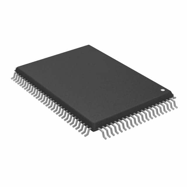
- Part No.:
- MC68EC020FG25
- Manufacturer:
- NXP Semiconductors
- Category:
- Microprocessors
- Package:
- 100-BQFP
- Datasheet:
-
 MC68EC020FG25.pdf
- Description:
- IC MPU M680X0 25MHZ 100QFP
- Quantity:
- Payment:

- Shipping:

Inventory:1,811
Please send an inquiry. Send us your inquiry, and we will respond immediately.
Product details
Overview
MC68EC020FG25 from Motorola is a 32-bit embedded microprocessor with 25 MHz maximum clock frequency, 256-byte on-chip instruction cache, and 32-bit address bus (A23–A0) supporting up to 16 MB physical memory space. It implements the full MC68000 family instruction set, features pipelined architecture, and operates in supervisor/user privilege modes - used in industrial controllers, legacy telecom equipment, and real-time embedded systems requiring deterministic interrupt response.
For engineers reviewing the MC68EC025 datasheet, MC68EC020FG25 pinout, MC68EC020FG25 application, or MC68EC020FG25 equivalent, key selection considerations include its reduced address bus width versus MC68020, absence of MMU, FG package thermal profile, and compatibility with 3.3 V or 5 V I/O interfaces depending on voltage mode configuration.
Technical Context
The MC68EC020FG25 executes instructions via a five-stage pipeline (fetch, decode, execute, memory access, write-back), supports dynamic bus sizing for 8/16/32-bit data transfers, and uses asynchronous bus control with DSACK0/DSACK1 handshaking. Its coprocessor interface enables concurrent operation with FPUs or custom accelerators using defined response primitives and CIR register set.
Unlike the full MC68020, the MC68EC020FG25 omits the MMU and reduces address bus to 24 bits (A23–A0), limiting physical addressing to 16 MB. It retains full 32-bit internal registers, 32-bit ALU, and identical exception vector table layout - enabling binary compatibility with MC68020 software when operating within its memory and peripheral constraints.
Key Specifications
| Parameter | Value and Actual Design Meaning |
|---|---|
| Max Clock Frequency | 25 MHz - defines maximum instruction throughput and synchronous peripheral timing budget |
| Address Bus Width | 24-bit (A23–A0) - supports 16 MB physical memory map, no external address multiplexing required |
| Data Bus Width | 32-bit (D31–D0) - enables single-cycle 32-bit operand fetch/store, reduces bus cycles for aligned data |
| On-Chip Instruction Cache | 256 bytes - improves average instruction fetch latency; no data cache present |
| Privilege Modes | Supervisor/User - enforces hardware-level protection for OS kernel and application code separation |
| Bus Arbitration | Three-wire protocol (BR, BG, BGACK) - allows coexistence with DMA controllers without external glue logic |
| Exception Vector Base | Fixed at 0x00000000 - simplifies vector table placement and boot ROM initialization |
Pinout & Package
MC68EC020FG25 is housed in a 132-pin ceramic PGA (Pin Grid Array) package with 0.1-inch pin spacing and 1.27 mm pitch. Thermal characteristics are optimized for convection-cooled industrial environments with θJA = 35°C/W.
| Pin/Terminal | Circuit Role | Design Meaning |
|---|---|---|
| CLK | Clock Input | Accepts TTL-compatible 25 MHz square wave; drives internal pipeline stages and bus timing generator |
| RESET | Asynchronous Reset | Forces CPU into initial state, clears pipeline, loads PC from vector 0; active-low, level-sensitive |
| AS | Address Strobe | Indicates valid address on A23–A0; synchronizes external memory/IO device address latching |
| DSACK0/DSACK1 | Data Strobe Acknowledge | Handshake signals confirming data bus readiness; support variable wait-state insertion by peripherals |
| BR/BG/BGACK | Bus Request/Grant/Acknowledge | Enables external DMA masters to seize bus control without CPU intervention or additional arbitration logic |
| FC2–FC0 | Function Code Outputs | Encode current bus cycle type (data, program, space) - critical for memory-mapped peripheral decoding |
| VCC/VSS | Power/Ground | Multiple dedicated pins per supply rail reduce IR drop and improve noise immunity in high-speed operation |
Key Features
| Feature | Design Value |
|---|---|
| Pipelined Execution Architecture | Five-stage pipeline enables overlapping instruction fetch/decode/execute - increases effective MIPS per MHz |
| 24-Bit Address Bus with Full 32-Bit ALU | Maintains 32-bit register width and arithmetic capability while reducing pin count and PCB routing complexity |
| On-Chip 256-Byte Instruction Cache | Reduces average instruction fetch time from external memory; no cache coherency logic required |
| Dedicated Coprocessor Interface | Supports concurrent FPU or custom accelerator operation using standardized command/response protocol and CIR register set |
| Asynchronous Bus Timing with DSACK | Allows interfacing with slow peripherals (e.g., UARTs, EEPROMs) without fixed wait states or clock division |
Applications
| Industrial Motion Controller | Legacy Telecom Switching Module |
|---|---|
Use Scenario: Real-time closed-loop servo control in CNC machines using analog I/O and encoder feedback. IC Role / Device Role / Timing Role: Main CPU executing deterministic control loops with sub-100 µs interrupt latency and precise timer-driven PWM generation. Use Value: Supervisor/user mode separation isolates firmware updates from runtime control tasks; 24-bit addressing suffices for onboard flash/RAM + peripheral register maps. | Use Scenario: Line card controller in TDM-based PBX systems managing channelized E1/T1 framing and signaling. IC Role / Device Role / Timing Role: Host processor handling HDLC framing, CAS/CCS signaling stacks, and time-slot assignment via memory-mapped FIFOs. Use Value: DSACK handshaking accommodates variable-latency FPGA-based framer logic; coprocessor interface enables optional DSP offload. |
| Avionics Display Processor | Medical Imaging Data Acquirer |
Use Scenario: Raster graphics rendering and overlay compositing in cockpit multifunction displays with discrete video DACs. IC Role / Device Role / Timing Role: Embedded controller managing frame buffer DMA, palette updates, and serial command interface to display panel. Use Value: 32-bit data bus enables fast pixel block transfers; fixed exception vector base simplifies DO-254-compliant boot sequence verification. | Use Scenario: Acquisition engine in ultrasound systems digitizing ADC streams and applying real-time beamforming coefficients. IC Role / Device Role / Timing Role: Real-time data orchestrator moving samples from dual-channel ADCs to SDRAM buffers and triggering FIR filter execution. Use Value: Three-wire bus arbitration allows simultaneous DMA capture and CPU processing without bus contention stalls. |
Equivalent & Alternatives
The following parts are listed as comparable options for similar embedded microprocessor applications.
| Alternative Part | Technical Difference | Application Difference | Selection Advice |
|---|---|---|---|
| MC68332ACFPE8 | Integrated QSM (Queued Serial Module), 16 MHz max, no external bus interface - monolithic MCU vs. MPU with external memory expansion | Suitable for self-contained control nodes; not viable for systems requiring >512 KB RAM or external peripherals via parallel bus | Select when system integration favors on-chip peripherals over flexibility of external memory mapping |
| SH7032 | 32-bit SuperH core, 20 MHz, 16 KB on-chip RAM, no external address/data bus - different ISA, no MC68K binary compatibility | Targets cost-sensitive consumer electronics; lacks MC68EC020's deterministic interrupt latency and bus arbitration protocol | Select only for green-field designs where software rewrites are acceptable and power efficiency outweighs legacy code reuse |
Compared with MC68EC020FG25, MC68332ACFPE8 trades external bus expandability for integrated peripherals and lower BOM count, while SH7032 abandons 68K compatibility entirely for higher IPC/MHz but requires full firmware porting.
Availability
MC68EC020FG25 is available at Aetrix Electronics and suitable for industrial motion controllers, legacy telecom switching modules, avionics display processors, and medical imaging data acquirers requiring stable component supply across extended product lifecycles.
Supply support for MC68EC020FG25 includes scheduled delivery planning, volume procurement assistance, BOM continuity management, traceable sourcing, and lifecycle availability coordination for OEM customers, industrial embedded developers, connected-device designers, and electronics production programs.
Manufacturer
Motorola Semiconductor (now NXP Semiconductors) was a pioneering U.S. semiconductor manufacturer known for the 68000 family, RF power transistors, and automotive ICs before its semiconductor division was acquired in 2004.
The MC68EC020 product line targets cost-optimized, memory-constrained embedded systems where full MMU functionality is unnecessary - emphasizing deterministic real-time behavior, bus arbitration for DMA coexistence, and long-term industrial temperature reliability.
FAQ
What is the maximum supported clock frequency for MC68EC020FG25?
The MC68EC020FG25 is rated for a maximum clock frequency of 25 MHz under specified industrial temperature and voltage conditions. This value is guaranteed by Motorola's AC electrical characteristics testing and defines the upper limit for reliable instruction execution, bus timing, and pipeline operation. Exceeding 25 MHz may result in timing violations, data corruption, or undefined behavior. The MC68EC020FG25 must be operated with a stable, low-jitter clock source meeting TTL input thresholds.
Does MC68EC020FG25 include an integrated memory management unit (MMU)?
No, the MC68EC020FG25 does not include an integrated MMU. Unlike the full MC68020, the EC variant omits the MMU to reduce die size, cost, and power consumption - making it suitable for real-time embedded applications that use flat memory models or rely on external memory controllers for protection. The MC68EC020FG25 retains supervisor/user privilege modes for basic software isolation but lacks virtual-to-physical address translation capabilities.
What package type and pin count does MC68EC020FG25 use?
The MC68EC020FG25 uses a 132-pin ceramic Pin Grid Array (PGA) package with 0.1-inch pin spacing and 1.27 mm pitch. This package is designated by the "FG" suffix and is thermally rated for industrial temperature range operation (–40°C to +85°C). The ceramic construction provides superior thermal stability and hermetic sealing compared to plastic packages, supporting long-term reliability in harsh environments where the MC68EC020FG25 is commonly deployed.
How does MC68EC020FG25 handle bus arbitration with DMA controllers?
The MC68EC020FG25 implements a three-wire bus arbitration protocol using BR (Bus Request), BG (Bus Grant), and BGACK (Bus Grant Acknowledge) signals. When an external DMA controller asserts BR, the MC68EC020FG25 completes its current bus cycle, releases AS and DSACK lines, and tri-states its address/data buses upon asserting BG. BGACK confirms bus ownership transfer. This protocol requires no external logic and is documented in Appendix A of the MC68EC020 user manual.
Is MC68EC020FG25 software-compatible with the MC68020?
Yes, the MC68EC020FG25 is binary-compatible with the MC68020 for all instructions and addressing modes, provided software operates within its 24-bit address space (16 MB) and does not invoke MMU-specific instructions (e.g., PFLUSH, PMOVE). Exception vectors, register set, pipeline behavior, and coprocessor interface are identical. Software written for MC68020 will run on MC68EC020FG25 without modification if memory map and peripheral access patterns respect the EC variant's architectural limits.
MC68EC020FG25 Specifications
- Product attributes
- Attribute value
- Manufacturer:
- NXP Semiconductors
- Package/Case:
- 100-BQFP
- Series:
- M680x0
- Packaging:
- Tray
- Product Status:
- Obsolete
- Core Processor:
- 68020
- Number of Cores/Bus Width:
- 1 Core, 32-Bit
- Speed:
- 25MHz
- Co-Processors/DSP:
- -
- RAM Controllers:
- -
- Graphics Acceleration:
- No
- Display & Interface Controllers:
- -
- Ethernet:
- -
- SATA:
- -
- USB:
- -
- Voltage - I/O:
- 5.0V
- Operating Temperature:
- 0°C ~ 70°C (TA)
- Grade:
- -
- Qualification:
- -
- Security Features:
- -
- Mounting Type:
- Surface Mount
- Supplier Device Package:
- 100-QFP (14x20)
- Additional Interfaces:
- -
MC68EC020FG25 FAQ
1.How can I place an order for MC68EC020FG25 through Aetrix?
Please submit a Request for Quotation (RFQ) for MC68EC020FG25 on Aetrix. Our sales agent will provide a competitive quotation and guide you through the order confirmation once you accept the terms.
2.Are the price and stock information for MC68EC020FG25 reliable?
The price and inventory of MC68EC020FG25 are updated periodically and may fluctuate due to market conditions. Stock and pricing data are typically refreshed every 24 hours. Quotation validity for MC68EC020FG25 is usually 5 days.
3.What payment methods are accepted for MC68EC020FG25?
We accept Wire Transfer, PayPal, Credit Card, Western Union, MoneyGram, and Escrow for MC68EC020FG25 transactions.
Note: Certain payment methods may incur a processing fee.
4.How is shipping managed for MC68EC020FG25?
MC68EC020FG25 orders can be shipped via leading logistics carriers, including DHL, UPS, FedEx, TNT, or Registered Mail.
Once your MC68EC020FG25 order is processed, you will receive an email with the shipment details and tracking number.
Note: Tracking information may take up to 24 hours to appear. Express delivery typically takes 3–5 business days.
5.How can I obtain technical support or documentation for MC68EC020FG25?
For technical support, including MC68EC020FG25 datasheets, pinout diagrams, or application guidance, please contact our engineering support team. They can provide detailed documentation and assistance for your MC68EC020FG25 requirements.
6.How does Aetrix verify that MC68EC020FG25 is sourced from the original manufacturer or authorized distributors?
All MC68EC020FG25 products on Aetrix are procured from qualified distributors and authorized channels. Our dedicated quality assurance team conducts strict verification, including traceability checks and, if necessary, third-party testing. This ensures that MC68EC020FG25 meets industry standards.
7.What is the process for return or replacement of MC68EC020FG25?
All MC68EC020FG25 units undergo pre-shipment inspection (PSI). If there is an issue with MC68EC020FG25, returns or replacements are accepted under the following conditions:
1.Quantity discrepancies, incorrect items, or visible external defects (such as breakage or corrosion), acknowledged by Aetrix.
2.The issue is reported within 90 days of delivery.
3.The MC68EC020FG25 part is unused and in its original packaging.
Return procedure for MC68EC020FG25:
1.Submit a request within 90 days.
2.Obtain a Return Material Authorization (RMA) from Aetrix.
MC68EC020FG25 Tags

-
AT91SAM9260B-CU-999
Microchip Technology
-
AT91SAM9G25-CU
Microchip Technology

-
ATSAMA5D27C-CU
Microchip Technology
-
AT91SAM9X35-CU
Microchip Technology
-
AT91SAM9X25-CU
Microchip Technology

-
MCIMX6Y2CVM08AB
NXP Semiconductors
.JPG)
-
AM3352BZCZ100
Texas Instruments
-
AT91SAM9260B-CU
Microchip Technology

-
AT91SAM9260B-QU
Microchip Technology

-
ATSAMA5D31A-CU
Microchip Technology
-
AT91SAM9G20B-CU-999
Microchip Technology
-
MCIMX6Y2CVM05AB
NXP Semiconductors
Tech Hub

A practical engineering guide to 3.3V and 5V logic compatibility, input thresholds, resistor dividers, translator ICs, MOSFET level shifting, I2C pull-ups, timing limits and power-sequencing risks.

The 74HC595 uses push-pull logic outputs, while the TPIC6B595 uses 50 V open-drain DMOS sinks for higher-power loads. This guide compares timing, current limits, 3.3 V interfacing, load wiring, thermal…

The 74HC595 converts serial data into eight stable parallel outputs. This guide covers pin functions, shift and storage timing, OE and MR behavior, drive-current limits, cascading, voltage compatibilit…

A technical comparison of level-sensitive latches and edge-triggered flip-flops, covering timing windows, setup and hold limits, master–slave operation, time borrowing, race-through, HDL inference and…

A D latch stores one bit while Enable controls when data can pass. This reference covers gate-level operation, truth tables, transparency, setup and hold timing, LE versus OE, common ICs and practical …

An SR latch stores one bit through cross-coupled feedback. This engineering reference covers NOR and NAND implementations, truth tables, forbidden-state recovery, gated operation, switch debouncing, fa…

Latch circuits retain one bit through feedback. This technical reference covers SR and D latches, truth tables, transparency, timing limits, latch-versus-flip-flop behavior, applications and common log…

An engineering guide to LED driver operation, constant-current and constant-voltage outputs, linear and switching topologies, dimming, IC selection, calculations, replacement compatibility, and fault c…

Operational amplifier guide covering op amp basics, feedback, ideal vs real op amps, common configurations, buffer circuits, offset, bias current, gain-bandwidth, slew rate, rail-to-rail limits and sel…

Jumper cables guide covering safe connection order, red and black clamp placement, final ground connection, cable gauge, length, clamp quality, copper vs CCA cables, jump starter comparison and battery…


