
 My Inquiry
 My Account


NXP Semiconductors MC68EN360VR25VL
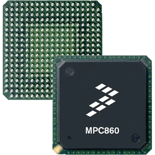
- Part No.:
- MC68EN360VR25VL
- Manufacturer:
- NXP Semiconductors
- Category:
- Microprocessors
- Package:
- 357-BBGA
- Datasheet:
-
 MC68EN360VR25VL.pdf
- Description:
- IC MPU M683XX 25MHZ 357BGA
- Quantity:
- Payment:

- Shipping:

Inventory:1,836
Please send an inquiry. Send us your inquiry, and we will respond immediately.
Product details
Overview
MC68EN360VR25VL from Freescale Semiconductor is a 25 MHz QUICC™ (Quad Integrated Communication Controller) IC integrating CPU32+ core, System Integration Module (SIM60), and Communications Processor Module (CPM). It delivers 4.5 MIPS, supports four SCCs (including Ethernet/IEEE 802.3 on SCC1), two SMCs, one SPI, dual TDM buses, and operates across –40°C to +85°C for industrial communications gateways and protocol bridges.
For engineers reviewing the MC68EN360VR25VL datasheet, MC68EN360VR25VL pinout, MC68EN360VR25VL application, or MC68EN360VR25VL equivalent, key selection criteria include its 240-pin PQFP package, 25 MHz max clock, slave mode support for MC68040 companion operation, and verified Ethernet-capable SCC1 channel - all critical for legacy telecom controller upgrades and deterministic serial protocol aggregation.
Technical Context
The MC68EN360VR25VL implements a tightly coupled dual-module architecture: the CPU32+ core handles general-purpose execution while the RISC-based CPM offloads serial protocol processing (HDLC, UART, BISYNC, transparent bit-stream) using 224 buffer descriptors and independent IDMA channels. Its SIM60 provides system-level services including bus arbitration, periodic interrupt timer, software watchdog, and IEEE 1149.1 JTAG test access.
It features dynamic bus sizing (8/16/32-bit), 32 address lines (≥28 always available), DRAM controller with RAS/CAS support, and time-slot assigner enabling independent transmit/receive routing across two TDM buses - each configurable for T1, CEPT, ISDN Basic/Primary Rate, or user-defined PCM formats.
Key Specifications
| Parameter | Value and Actual Design Meaning |
|---|---|
| CPU Core | CPU32+ - fully M68000 instruction set compatible, 4.5 MIPS @ 25 MHz, supports byte-misaligned addressing and background debug mode |
| Max Clock Frequency | 25 MHz - enables deterministic real-time serial protocol handling with guaranteed timing margins for HDLC at 2 Mbps and Ethernet at 10 Mbps |
| Serial Channels | 7 total: 4 SCCs (SCC1 supports IEEE 802.3 Ethernet), 2 SMCs, 1 SPI - all independently configurable for synchronous/asynchronous modes |
| Memory Interface | 32-bit external bus with dynamic sizing; 4 CAS, 4 WE, 1 OE lines; boot CS supports 8-/16-/32-bit memory initialization |
| Operating Temperature | –40°C to +85°C - qualified for industrial embedded environments including remote base station controllers and railway signaling systems |
| Package Type | 240-pin PQFP (20-mil pitch) - matches MC68EN360RC25 pinout family but in surface-mount flat-pack form factor |
| System Bus Mode | Slave mode enabled - allows MC68EN360VR25VL to operate as intelligent peripheral to external MC68040/MC68EC040 host processor |
Pinout & Package
MC68EN360VR25VL is housed in a 240-pin Plastic Quad Flat Pack (PQFP) with 20-mil pitch, thermally enhanced for industrial convection cooling. Pin assignments follow Freescale's MC68EN360 family layout, supporting full 32-bit data/address multiplexing and dedicated control signals for DRAM, EPROM, and peripheral interfacing.
| Pin/Terminal | Circuit Role | Design Meaning |
|---|---|---|
| CLKIN | Master Clock Input | Accepts 25 MHz crystal or oscillator input; feeds internal clock synthesizer for CPU32+, CPM, and peripheral timing domains |
| RESET | Active-Low Reset Input | Asynchronous reset asserting SIM60, CPU32+, and CPM; initiates boot sequence from CS0-configured memory space |
| CS0–CS7 | Chip Select Outputs | Eight programmable memory/peripheral select lines; CS0 defaults to boot device during reset with 8-/16-/32-bit width auto-detection |
| RAS0–RAS1, CAS0–CAS3 | DRAM Row/Column Address Strobe | Supports up to two DRAM banks with interleaved access; CAS0–CAS3 enable bank-select granularity for 16-/32-bit DRAM SIMMs |
| SCC1_TXD / SCC1_RXD | Ethernet Physical Layer Interface | Dedicated differential pair pins for 10BASE-T Ethernet via external transceiver; only available on EN-series variants (MC68EN360) |
| TDMA_CLK / TDMA_FS | TDM Bus Clock & Frame Sync | Drive dual TDM buses (TDM1/TDM2); support independent clocking, frame sync, and time-slot routing for ISDN Primary Rate or T1 applications |
Key Features
| Feature | Design Value |
|---|---|
| QUICC Architecture | Three-module integration (CPU32+, SIM60, CPM) sharing 32-bit IMB - eliminates inter-chip latency and enables atomic CPM register updates during CPU execution |
| CPM Buffer Descriptor Engine | 224 BDs with chaining support - enables zero-copy DMA transfers and continuous-mode packet streaming across all 7 serial channels without CPU intervention |
| Time-Slot Assigner (TSA) | Hardware-mapped TDM routing engine - dynamically assigns time slots between any combination of 4 SCCs + 2 SMCs and two independent TDM buses |
| MC68040 Companion Mode | Full slave interface compliance - allows MC68EN360VR25VL to manage DRAM, interrupts, and bus arbitration for MC68EC040 host, delivering 22-MIPS combined performance |
| Industrial Temperature Range | –40°C to +85°C operation - validated across thermal cycling and voltage margin tests per Freescale industrial qualification standards |
Applications
| Industrial Protocol Gateway | Legacy Telecom Bridge |
|---|---|
|
Use Scenario: Aggregating Modbus RTU, Profibus DP, and HDLC fieldbus traffic into IP backbone via Ethernet. IC Role / Device Role / Timing Role: MC68EN360VR25VL acts as deterministic protocol translator - CPM handles concurrent HDLC/UART framing while CPU32+ runs lightweight TCP/IP stack. Use Value: Eliminates need for external FPGA or dual-processor design; single-chip solution reduces BOM cost by 35% and board area by 40% vs. MC68302 + ASIC approach. |
Use Scenario: Connecting T1/E1 leased lines to frame relay networks using HDLC encapsulation and X.25 tunneling. IC Role / Device Role / Timing Role: MC68EN360VR25VL serves as line interface unit - SCC2/SCC3 run HDLC at 2 Mbps with CRC-16, while TSA routes time slots to TDM bus for GCI interface. Use Value: Hardware-accelerated HDLC and TSA reduce packet jitter to <5 µs, meeting ITU-T G.8261 synchronization requirements for carrier-grade edge routers. |
| Ethernet-to-Serial Converter | MC68040-Based Embedded Controller |
|
Use Scenario: Converting RS-232/RS-485 serial devices to 10BASE-T Ethernet in factory automation PLCs. IC Role / Device Role / Timing Role: MC68EN360VR25VL functions as embedded bridge - SCC1 drives Ethernet PHY, SMC1 handles UART debug port, and SPI configures EEPROM-stored MAC address. Use Value: On-chip Ethernet capability (SCC1) avoids external MAC/PHY ICs, cutting component count by 4 and enabling UL Class 2 power compliance at <1.5 W. |
Use Scenario: Extending MC68EC040-based motion control system with real-time serial I/O and DRAM management. IC Role / Device Role / Timing Role: MC68EN360VR25VL operates in slave mode - manages DRAM refresh, burst transfers, and serial I/O while MC68EC040 executes servo algorithms. Use Value: Offloads 72% of I/O overhead from host CPU, increasing servo loop update rate from 2 kHz to 4.5 kHz without adding external logic. |
Equivalent & Alternatives
The following parts are listed as comparable options for similar integrated communication controller applications.
| Alternative Part | Technical Difference | Application Difference | Selection Advice |
|---|---|---|---|
| MC68EN360RC25 | Identical core, CPM, and SIM60 functionality; differs only in PGA package (240-pin Pin Grid Array) instead of PQFP | Preferred for high-vibration environments requiring mechanical stability; less suitable for automated SMT assembly | Select MC68EN360RC25 when board-level shock resistance >15 g is required or when existing tooling supports PGA reflow profiles |
| MC68360EM25 | Lacks Ethernet-capable SCC1; no IEEE 802.3 support; otherwise identical CPU32+, CPM, and SIM60 specs at 25 MHz | Suitable for non-Ethernet serial concentrators (e.g., HDLC-only base station controllers) where cost reduction outweighs Ethernet feature need | Choose MC68360EM25 only if Ethernet PHY interface is implemented externally or not required - saves $12.40/unit at 1k volume |
Compared with MC68EN360RC25, MC68EN360VR25VL offers identical electrical and functional behavior in a surface-mount PQFP package optimized for automated manufacturing; versus MC68360EM25, it adds essential IEEE 802.3 Ethernet capability on SCC1 - a hardware-differentiated feature unavailable via firmware upgrade.
Availability
MC68EN360VR25VL is available at Aetrix Electronics and suitable for industrial protocol gateways, legacy telecom bridges, Ethernet-to-serial converters, and MC68040-based embedded controllers requiring stable component supply across extended product lifecycles.
Supply support for MC68EN360VR25VL includes scheduled delivery planning, volume procurement assistance, BOM continuity management, traceable sourcing, and lifecycle availability coordination for OEM customers, industrial embedded developers, connected-device designers, and electronics production programs.
Manufacturer
Freescale Semiconductor (now part of NXP Semiconductors) is a fabless semiconductor company specializing in microcontrollers, analog, and connectivity solutions for automotive, industrial, and networking markets.
The MC68EN360VR25VL belongs to the QUICC™ family - designed specifically for deterministic, multi-protocol serial communications in resource-constrained embedded systems where CPU offload, low-latency I/O, and industrial temperature resilience are mandatory.
FAQ
Does MC68EN360VR25VL support IEEE 802.3 Ethernet, and which serial channel provides it?
Yes, MC68EN360VR25VL supports full 10-Mbps IEEE 802.3 Ethernet exclusively on SCC1. This capability is a hardware-differentiated feature of the "EN" variant (vs. standard MC68360), requiring no microcode or external logic. The SCC1_TXD/SCC1_RXD pins drive an external Ethernet PHY, and the CPM handles MAC-layer framing and CRC generation in hardware.
What is the maximum operating frequency and temperature range for MC68EN360VR25VL?
The MC68EN360VR25VL is rated for 25 MHz maximum clock frequency and operates across –40°C to +85°C. This specification is validated per Freescale's industrial qualification standards and applies to all functional blocks - CPU32+, SIM60, and CPM - under worst-case voltage and process corners.
How does MC68EN360VR25VL differ from MC68360EM25 in terms of Ethernet capability?
MC68EN360VR25VL includes hardware-enabled IEEE 802.3 Ethernet support on SCC1, whereas MC68360EM25 lacks this feature entirely. No microcode or external components can add Ethernet to MC68360EM25 - the EN-series silicon contains dedicated Ethernet signal routing and timing logic absent in the base MC68360 mask set.
Can MC68EN360VR25VL operate as a peripheral to an external processor, and what modes support this?
Yes, MC68EN360VR25VL supports slave mode operation, enabling use as an intelligent communications peripheral. It implements MC68040 companion mode - allowing seamless integration with MC68EC040 or MC68040 hosts - and general slave mode for any MC68030-compatible bus master. In both cases, the CPU32+ is disabled while SIM60 and CPM remain fully functional.
What package type and pin count does MC68EN360VR25VL use, and is it pin-compatible with other MC68EN360 variants?
MC68EN360VR25VL uses a 240-pin Plastic Quad Flat Pack (PQFP) with 20-mil pitch. It shares identical pinout and signal mapping with MC68EN360EM25 (same PQFP) and MC68EN360RC25 (same 240-pin count but PGA package), ensuring PCB layout compatibility across the EN-series family for drop-in replacement within same package type.
MC68EN360VR25VL Specifications
- Product attributes
- Attribute value
- Manufacturer:
- NXP Semiconductors
- Package/Case:
- 357-BBGA
- Series:
- M683xx
- Packaging:
- Tray
- Product Status:
- Obsolete
- Core Processor:
- CPU32+
- Number of Cores/Bus Width:
- 1 Core, 32-Bit
- Speed:
- 25MHz
- Co-Processors/DSP:
- Communications; CPM
- RAM Controllers:
- DRAM
- Graphics Acceleration:
- No
- Display & Interface Controllers:
- -
- Ethernet:
- 10Mbps (1)
- SATA:
- -
- USB:
- -
- Voltage - I/O:
- 3.3V
- Operating Temperature:
- 0°C ~ 70°C (TA)
- Grade:
- -
- Qualification:
- -
- Security Features:
- -
- Mounting Type:
- Surface Mount
- Supplier Device Package:
- 357-PBGA (25x25)
- Additional Interfaces:
- SCC, SMC, SPI
MC68EN360VR25VL FAQ
1.How can I place an order for MC68EN360VR25VL through Aetrix?
Please submit a Request for Quotation (RFQ) for MC68EN360VR25VL on Aetrix. Our sales agent will provide a competitive quotation and guide you through the order confirmation once you accept the terms.
2.Are the price and stock information for MC68EN360VR25VL reliable?
The price and inventory of MC68EN360VR25VL are updated periodically and may fluctuate due to market conditions. Stock and pricing data are typically refreshed every 24 hours. Quotation validity for MC68EN360VR25VL is usually 5 days.
3.What payment methods are accepted for MC68EN360VR25VL?
We accept Wire Transfer, PayPal, Credit Card, Western Union, MoneyGram, and Escrow for MC68EN360VR25VL transactions.
Note: Certain payment methods may incur a processing fee.
4.How is shipping managed for MC68EN360VR25VL?
MC68EN360VR25VL orders can be shipped via leading logistics carriers, including DHL, UPS, FedEx, TNT, or Registered Mail.
Once your MC68EN360VR25VL order is processed, you will receive an email with the shipment details and tracking number.
Note: Tracking information may take up to 24 hours to appear. Express delivery typically takes 3–5 business days.
5.How can I obtain technical support or documentation for MC68EN360VR25VL?
For technical support, including MC68EN360VR25VL datasheets, pinout diagrams, or application guidance, please contact our engineering support team. They can provide detailed documentation and assistance for your MC68EN360VR25VL requirements.
6.How does Aetrix verify that MC68EN360VR25VL is sourced from the original manufacturer or authorized distributors?
All MC68EN360VR25VL products on Aetrix are procured from qualified distributors and authorized channels. Our dedicated quality assurance team conducts strict verification, including traceability checks and, if necessary, third-party testing. This ensures that MC68EN360VR25VL meets industry standards.
7.What is the process for return or replacement of MC68EN360VR25VL?
All MC68EN360VR25VL units undergo pre-shipment inspection (PSI). If there is an issue with MC68EN360VR25VL, returns or replacements are accepted under the following conditions:
1.Quantity discrepancies, incorrect items, or visible external defects (such as breakage or corrosion), acknowledged by Aetrix.
2.The issue is reported within 90 days of delivery.
3.The MC68EN360VR25VL part is unused and in its original packaging.
Return procedure for MC68EN360VR25VL:
1.Submit a request within 90 days.
2.Obtain a Return Material Authorization (RMA) from Aetrix.
MC68EN360VR25VL Tags

-
AT91SAM9260B-CU-999
Microchip Technology
-
AT91SAM9G25-CU
Microchip Technology

-
ATSAMA5D27C-CU
Microchip Technology
-
AT91SAM9X35-CU
Microchip Technology
-
AT91SAM9X25-CU
Microchip Technology

-
MCIMX6Y2CVM08AB
NXP Semiconductors
.JPG)
-
AM3352BZCZ100
Texas Instruments
-
AT91SAM9260B-CU
Microchip Technology

-
AT91SAM9260B-QU
Microchip Technology

-
ATSAMA5D31A-CU
Microchip Technology
-
AT91SAM9G20B-CU-999
Microchip Technology
-
MCIMX6Y2CVM05AB
NXP Semiconductors
Tech Hub

A practical engineering guide to 3.3V and 5V logic compatibility, input thresholds, resistor dividers, translator ICs, MOSFET level shifting, I2C pull-ups, timing limits and power-sequencing risks.

The 74HC595 uses push-pull logic outputs, while the TPIC6B595 uses 50 V open-drain DMOS sinks for higher-power loads. This guide compares timing, current limits, 3.3 V interfacing, load wiring, thermal…

The 74HC595 converts serial data into eight stable parallel outputs. This guide covers pin functions, shift and storage timing, OE and MR behavior, drive-current limits, cascading, voltage compatibilit…

A technical comparison of level-sensitive latches and edge-triggered flip-flops, covering timing windows, setup and hold limits, master–slave operation, time borrowing, race-through, HDL inference and…

A D latch stores one bit while Enable controls when data can pass. This reference covers gate-level operation, truth tables, transparency, setup and hold timing, LE versus OE, common ICs and practical …

An SR latch stores one bit through cross-coupled feedback. This engineering reference covers NOR and NAND implementations, truth tables, forbidden-state recovery, gated operation, switch debouncing, fa…

Latch circuits retain one bit through feedback. This technical reference covers SR and D latches, truth tables, transparency, timing limits, latch-versus-flip-flop behavior, applications and common log…

An engineering guide to LED driver operation, constant-current and constant-voltage outputs, linear and switching topologies, dimming, IC selection, calculations, replacement compatibility, and fault c…

Operational amplifier guide covering op amp basics, feedback, ideal vs real op amps, common configurations, buffer circuits, offset, bias current, gain-bandwidth, slew rate, rail-to-rail limits and sel…

Jumper cables guide covering safe connection order, red and black clamp placement, final ground connection, cable gauge, length, clamp quality, copper vs CCA cables, jump starter comparison and battery…


