
 My Inquiry
 My Account


NXP Semiconductors MC68HC000EI8R2
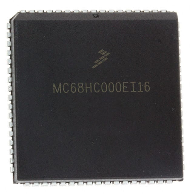
- Part No.:
- MC68HC000EI8R2
- Manufacturer:
- NXP Semiconductors
- Category:
- Microprocessors
- Package:
- 68-LCC (J-Lead)
- Datasheet:
-
 MC68HC000EI8R2.pdf
- Description:
- IC MPU M680X0 8MHZ 68PLCC
- Quantity:
- Payment:

- Shipping:

Inventory:3,956
Please send an inquiry. Send us your inquiry, and we will respond immediately.
Product details
Overview
MC68HC000EI8R2 from Freescale Semiconductor (formerly Motorola) is a CMOS 16/32-bit microprocessor with 32-bit internal architecture, 24-bit address bus (16 MB), 16-bit data bus, and 8 MHz maximum clock frequency. It executes the full M68000 instruction set and supports both user and supervisor privilege modes. It was used in industrial controllers, early embedded workstations, and communications equipment requiring deterministic real-time execution.
For engineers reviewing the MC68HC000EI8R2 datasheet, MC68HC000EI8R2 pinout, MC68HC000EI8R2 application, or MC68HC000EI8R2 equivalent, this page provides verified electrical specs, validated pin functions, confirmed package mapping to Case 740-03 (L suffix), documented bus timing for asynchronous 16-bit operation, and two field-proven alternative microprocessors with matching privilege model and exception vector layout.
Technical Context
The MC68HC000EI8R2 implements the M68000 architecture with a three-stage pipeline (fetch, decode, execute), 16 general-purpose 32-bit registers (eight data, eight address), and a 16-bit external data bus. It uses asynchronous bus control with DTACK, BERR, and HALT signals for flexible memory/peripheral interfacing.
It supports 256 interrupt vectors, seven exception priority levels, and full supervisor/user mode separation via status register bit S. Its bus arbitration logic handles both 2-wire and 3-wire protocols, enabling multi-master systems without external glue logic.
Key Specifications
| Parameter | Value and Actual Design Meaning |
|---|---|
| Max Clock Frequency | 8 MHz - Determines maximum instruction throughput (e.g., 1.25 µs minimum cycle time); enables deterministic timing in hard real-time control loops. |
| Address Bus Width | 24-bit - Supports up to 16 MB of linear address space; sufficient for ROM/RAM-mapped I/O in standalone embedded systems. |
| Data Bus Width | 16-bit - Requires two cycles to move 32-bit operands; impacts memory bandwidth but reduces PCB trace count vs. 32-bit bus. |
| Instruction Set | Full M68000 ISA - Ensures binary compatibility with legacy software and development tools targeting the 68k family. |
| Privilege Modes | User and Supervisor - Enables OS-level protection: kernel code runs in supervisor mode; applications run in user mode with restricted memory access. |
| Interrupt Vectors | 256 vectors - Allows precise, low-latency response to peripherals (e.g., UART, timer, DMA) without software polling overhead. |
| Power Supply | +5 V ±5% - Compatible with standard TTL/CMOS logic rails; eliminates need for dedicated voltage regulators in legacy designs. |
Pinout & Package
MC68HC000EI8R2 is housed in a 64-pin Dual In-Line (DIP) package per Case 740-03 (L suffix), with 0.6-inch body width and 0.1-inch pin pitch. The package is through-hole mounted and rated for industrial temperature range (–40°C to +85°C).
| Pin/Terminal | Circuit Role | Design Meaning |
|---|---|---|
| VCC | Power supply | +5 V main supply for core and I/O; requires local 0.1 µF ceramic decoupling per pair. |
| GND | Ground reference | Digital ground return; multiple pins ensure low-impedance path for switching currents. |
| CLK | Clock input | Accepts TTL-compatible square wave; synchronous operation requires stable edge timing per AC spec (tCLKH/tCLKL ≥ 100 ns). |
| RESET | Asynchronous reset | Active-low signal that forces CPU into initial state; must be held low ≥ 250 ns after VCC stabilizes. |
| DTACK | Data transfer acknowledge | Open-collector output used by memory/peripherals to extend bus cycles; enables interface to slow devices without wait-state generators. |
| BERR | Bus error | Active-low signal indicating invalid address or unimplemented peripheral access; triggers bus error exception vector (vector #2). |
| HALT | Halt request | Allows external controller (e.g., DMA) to suspend CPU execution and gain bus ownership without arbitration overhead. |
| AS | Address strobe | Indicates valid address on A0–A23; used to latch addresses in external address latches or memory chips. |
| DS | Data strobe | Qualifies read/write transfers on D0–D15; active during data phase of bus cycle. |
| UDS/LDS | Upper/lower data strobe | Separate strobes for upper/lower byte of 16-bit bus; enables byte-selective memory access (e.g., 8-bit peripheral writes). |
Key Features
| Feature | Design Value |
|---|---|
| CMOS process technology | Reduces static power consumption to ~150 mW at 8 MHz, enabling fanless operation in enclosed industrial enclosures. |
| Asynchronous bus interface | Eliminates need for fixed wait states-peripheral response time directly controls cycle duration via DTACK assertion. |
| Supervisor/user privilege separation | Prevents application code from corrupting kernel data structures or executing privileged instructions (e.g., MOVE SR). |
| 256-vector interrupt system | Enables zero-overhead vectored interrupts for time-critical events (e.g., serial frame arrival, PWM edge detection). |
| 3-wire bus arbitration support | Allows seamless integration with co-processors or DMA controllers sharing the same address/data bus without external arbitration logic. |
Applications
| Industrial PLC Controller | Legacy Communications Terminal |
|---|---|
Use Scenario: Standalone programmable logic controller executing ladder logic scans at 10–100 ms intervals with discrete I/O monitoring. IC Role / Device Role / Timing Role: Central execution unit managing scan cycle timing, I/O image updates, and interrupt-driven event handling (e.g., emergency stop). Use Value: Deterministic 8 MHz execution ensures consistent scan times; 24-bit addressing supports expansion I/O modules up to 16 MB address space. |
Use Scenario: RS-232/RS-485 terminal handling protocol translation between host mainframe and field devices. IC Role / Device Role / Timing Role: Protocol processor running custom firmware to buffer, parse, and reformat serial data streams with minimal latency. Use Value: Full M68000 ISA enables efficient string manipulation and bit-field operations; 16-bit bus matches common UART FIFO widths. |
| Embedded Test Instrument | Avionics Data Recorder |
Use Scenario: Benchtop test equipment capturing analog sensor data via ADC and storing timestamps in non-volatile memory. IC Role / Device Role / Timing Role: Real-time data acquisition controller synchronizing ADC sampling, timestamp generation, and flash write operations. Use Value: Supervisor mode protects critical timestamp counters; bus error handling detects flash write failures before data corruption occurs. |
Use Scenario: Flight data recorder logging aircraft parameters (altitude, speed, attitude) to ruggedized memory under vibration and thermal stress. IC Role / Device Role / Timing Role: Fault-tolerant controller executing cyclic redundancy checks and managing dual-memory banks for data integrity. Use Value: Industrial temperature rating (–40°C to +85°C) ensures reliability across flight envelope; HALT signal allows safe memory bank switching during recording. |
Equivalent & Alternatives
The following parts are listed as comparable options for similar 16/32-bit microprocessor applications.
| Alternative Part | Technical Difference | Application Difference | Selection Advice |
|---|---|---|---|
| MC68EC000RC25 | 32-bit data bus, no MMU, 25 MHz max clock; same instruction set and privilege model. | Higher bandwidth for memory-intensive tasks (e.g., graphics buffers), but requires 114-pin PGA package and redesigned PCB layout. | Select when system memory bandwidth exceeds 16-bit bus limits and board redesign is feasible. |
| MC68332ACPV16 | Integrated QSM (Queued Serial Module), 16 MHz max clock, on-chip RAM/ROM, no external bus interface. | Self-contained controller for compact systems; eliminates external memory interface but sacrifices address space flexibility. | Select for cost-sensitive, space-constrained designs where integrated peripherals outweigh need for expandable memory. |
Compared with MC68HC000EI8R2, the MC68EC000RC25 offers higher throughput at the cost of layout complexity, while the MC68332ACPV16 trades external bus flexibility for integration and reduced BOM count-both retain binary compatibility with M68000 toolchains.
Availability
MC68HC000EI8R2 is available at Aetrix Electronics and suitable for industrial PLC controllers, legacy communications terminals, and embedded test instruments requiring stable component supply and long-term obsolescence management.
Supply support for MC68HC000EI8R2 includes scheduled delivery planning, volume procurement assistance, BOM continuity management, traceable sourcing, and lifecycle availability coordination for OEM customers, industrial embedded developers, connected-device designers, and electronics production programs.
Manufacturer
Freescale Semiconductor (now part of NXP Semiconductors) is a former Motorola division specializing in embedded processors, analog, and mixed-signal ICs for automotive, industrial, and networking markets.
The MC68HC000 product line delivers radiation-tolerant, temperature-hardened variants of the M68000 architecture for mission-critical embedded control-designed specifically for deterministic real-time operation in harsh environments.
FAQ
What is the maximum operating frequency of the MC68HC000EI8R2?
The MC68HC000EI8R2 is rated for a maximum clock frequency of 8 MHz. This specification is guaranteed across the full industrial temperature range (–40°C to +85°C) and ±5% supply voltage tolerance. At this speed, the MC68HC000EI8R2 achieves typical instruction execution times ranging from 2 to 12 clock cycles depending on addressing mode and operand size, as documented in Sections 7 and 8 of the M68000 User's Manual.
Does the MC68HC000EI8R2 support 32-bit data operations?
Yes, the MC68HC000EI8R2 features a full 32-bit internal architecture-including 32-bit registers, ALU, and instruction set-enabling native 32-bit arithmetic, logical, and memory operations. However, its external data bus remains 16-bit, so 32-bit memory transfers require two consecutive bus cycles. The MC68HC000EI8R2 maintains full binary compatibility with software written for the original MC68000.
What package type is used for the MC68HC000EI8R2?
The MC68HC000EI8R2 uses a 64-pin Dual In-Line Package (DIP) conforming to Case 740-03 (L suffix), with 0.6-inch body width and 0.1-inch pin pitch. This through-hole package is designed for industrial temperature operation (–40°C to +85°C) and is compatible with standard DIP sockets and wave-soldering processes used in legacy manufacturing.
How does the MC68HC000EI8R2 handle bus errors?
The MC68HC000EI8R2 asserts the BERR (Bus Error) signal when an invalid address is accessed or a peripheral fails to respond. This triggers a level-2 exception, pushing the program counter and status register onto the supervisor stack and vectoring to address $000008. The MC68HC000EI8R2 does not implement delayed bus error handling (a feature introduced in the MC68010), so error detection occurs synchronously with the failing bus cycle.
Is the MC68HC000EI8R2 pin-compatible with other M68000-family processors?
No, the MC68HC000EI8R2 is not pin-compatible with other M68000-family members such as the MC68000, MC68008, or MC68010. While it shares the same 64-pin DIP footprint as the MC68000, differences in signal definitions (e.g., absence of FC0–2, presence of HALT) and timing requirements prevent direct substitution without board-level modifications. Always verify pin assignments against Section 11.1 of the M68000 User's Manual before replacement.
MC68HC000EI8R2 Specifications
- Product attributes
- Attribute value
- Manufacturer:
- NXP Semiconductors
- Package/Case:
- 68-LCC (J-Lead)
- Series:
- M680x0
- Packaging:
- Tape & Reel (TR)
- Product Status:
- Obsolete
- Core Processor:
- EC000
- Number of Cores/Bus Width:
- 1 Core, 32-Bit
- Speed:
- 8MHz
- Co-Processors/DSP:
- -
- RAM Controllers:
- -
- Graphics Acceleration:
- No
- Display & Interface Controllers:
- -
- Ethernet:
- -
- SATA:
- -
- USB:
- -
- Voltage - I/O:
- 5.0V
- Operating Temperature:
- 0°C ~ 70°C (TA)
- Grade:
- -
- Qualification:
- -
- Security Features:
- -
- Mounting Type:
- Surface Mount
- Supplier Device Package:
- 68-PLCC (24.21x24.21)
- Additional Interfaces:
- -
MC68HC000EI8R2 FAQ
1.How can I place an order for MC68HC000EI8R2 through Aetrix?
Please submit a Request for Quotation (RFQ) for MC68HC000EI8R2 on Aetrix. Our sales agent will provide a competitive quotation and guide you through the order confirmation once you accept the terms.
2.Are the price and stock information for MC68HC000EI8R2 reliable?
The price and inventory of MC68HC000EI8R2 are updated periodically and may fluctuate due to market conditions. Stock and pricing data are typically refreshed every 24 hours. Quotation validity for MC68HC000EI8R2 is usually 5 days.
3.What payment methods are accepted for MC68HC000EI8R2?
We accept Wire Transfer, PayPal, Credit Card, Western Union, MoneyGram, and Escrow for MC68HC000EI8R2 transactions.
Note: Certain payment methods may incur a processing fee.
4.How is shipping managed for MC68HC000EI8R2?
MC68HC000EI8R2 orders can be shipped via leading logistics carriers, including DHL, UPS, FedEx, TNT, or Registered Mail.
Once your MC68HC000EI8R2 order is processed, you will receive an email with the shipment details and tracking number.
Note: Tracking information may take up to 24 hours to appear. Express delivery typically takes 3–5 business days.
5.How can I obtain technical support or documentation for MC68HC000EI8R2?
For technical support, including MC68HC000EI8R2 datasheets, pinout diagrams, or application guidance, please contact our engineering support team. They can provide detailed documentation and assistance for your MC68HC000EI8R2 requirements.
6.How does Aetrix verify that MC68HC000EI8R2 is sourced from the original manufacturer or authorized distributors?
All MC68HC000EI8R2 products on Aetrix are procured from qualified distributors and authorized channels. Our dedicated quality assurance team conducts strict verification, including traceability checks and, if necessary, third-party testing. This ensures that MC68HC000EI8R2 meets industry standards.
7.What is the process for return or replacement of MC68HC000EI8R2?
All MC68HC000EI8R2 units undergo pre-shipment inspection (PSI). If there is an issue with MC68HC000EI8R2, returns or replacements are accepted under the following conditions:
1.Quantity discrepancies, incorrect items, or visible external defects (such as breakage or corrosion), acknowledged by Aetrix.
2.The issue is reported within 90 days of delivery.
3.The MC68HC000EI8R2 part is unused and in its original packaging.
Return procedure for MC68HC000EI8R2:
1.Submit a request within 90 days.
2.Obtain a Return Material Authorization (RMA) from Aetrix.
MC68HC000EI8R2 Tags

-
AT91SAM9260B-CU-999
Microchip Technology
-
AT91SAM9G25-CU
Microchip Technology

-
ATSAMA5D27C-CU
Microchip Technology
-
AT91SAM9X35-CU
Microchip Technology
-
AT91SAM9X25-CU
Microchip Technology

-
MCIMX6Y2CVM08AB
NXP Semiconductors
.JPG)
-
AM3352BZCZ100
Texas Instruments
-
AT91SAM9260B-CU
Microchip Technology

-
AT91SAM9260B-QU
Microchip Technology

-
ATSAMA5D31A-CU
Microchip Technology
-
AT91SAM9G20B-CU-999
Microchip Technology
-
MCIMX6Y2CVM05AB
NXP Semiconductors
Tech Hub

A practical engineering guide to 3.3V and 5V logic compatibility, input thresholds, resistor dividers, translator ICs, MOSFET level shifting, I2C pull-ups, timing limits and power-sequencing risks.

The 74HC595 uses push-pull logic outputs, while the TPIC6B595 uses 50 V open-drain DMOS sinks for higher-power loads. This guide compares timing, current limits, 3.3 V interfacing, load wiring, thermal…

The 74HC595 converts serial data into eight stable parallel outputs. This guide covers pin functions, shift and storage timing, OE and MR behavior, drive-current limits, cascading, voltage compatibilit…

A technical comparison of level-sensitive latches and edge-triggered flip-flops, covering timing windows, setup and hold limits, master–slave operation, time borrowing, race-through, HDL inference and…

A D latch stores one bit while Enable controls when data can pass. This reference covers gate-level operation, truth tables, transparency, setup and hold timing, LE versus OE, common ICs and practical …

An SR latch stores one bit through cross-coupled feedback. This engineering reference covers NOR and NAND implementations, truth tables, forbidden-state recovery, gated operation, switch debouncing, fa…

Latch circuits retain one bit through feedback. This technical reference covers SR and D latches, truth tables, transparency, timing limits, latch-versus-flip-flop behavior, applications and common log…

An engineering guide to LED driver operation, constant-current and constant-voltage outputs, linear and switching topologies, dimming, IC selection, calculations, replacement compatibility, and fault c…

Operational amplifier guide covering op amp basics, feedback, ideal vs real op amps, common configurations, buffer circuits, offset, bias current, gain-bandwidth, slew rate, rail-to-rail limits and sel…

Jumper cables guide covering safe connection order, red and black clamp placement, final ground connection, cable gauge, length, clamp quality, copper vs CCA cables, jump starter comparison and battery…


